Ten Factors that Influence the Cost of QCM-D Systems
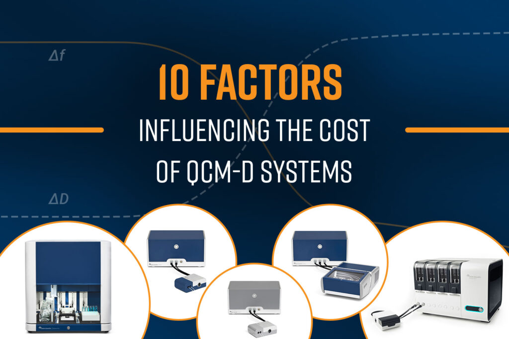
Quartz crystal microbalance with dissipation monitoring (QCM-D) instruments are powerful tools for real-time, label-free analysis of molecular interactions on a surface in a liquid environment. QCM-D systems can quantify nanoscale mass changes and viscoelastic properties of thin films on the surface in adsorption or desorption studies., If you are curious about adding QCM-D to your […]
The Hidden Costs of Polymer Compounding in R&D
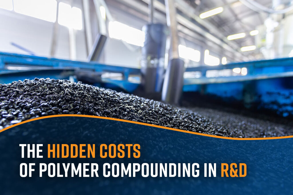
Polymer compounding is fundamental to developing new polymeric materials in sectors such as automotive, aerospace, medical devices, and packaging. While traditional compounding methods remain prevalent in research and development (R&D) environments, they often come with hidden costs that impact time and resources. What Is Traditional Polymer Compounding? Traditional polymer compounding usually operates on industrial principles […]
2-Day SEM Short Course | Alexandria, VA | April 2026
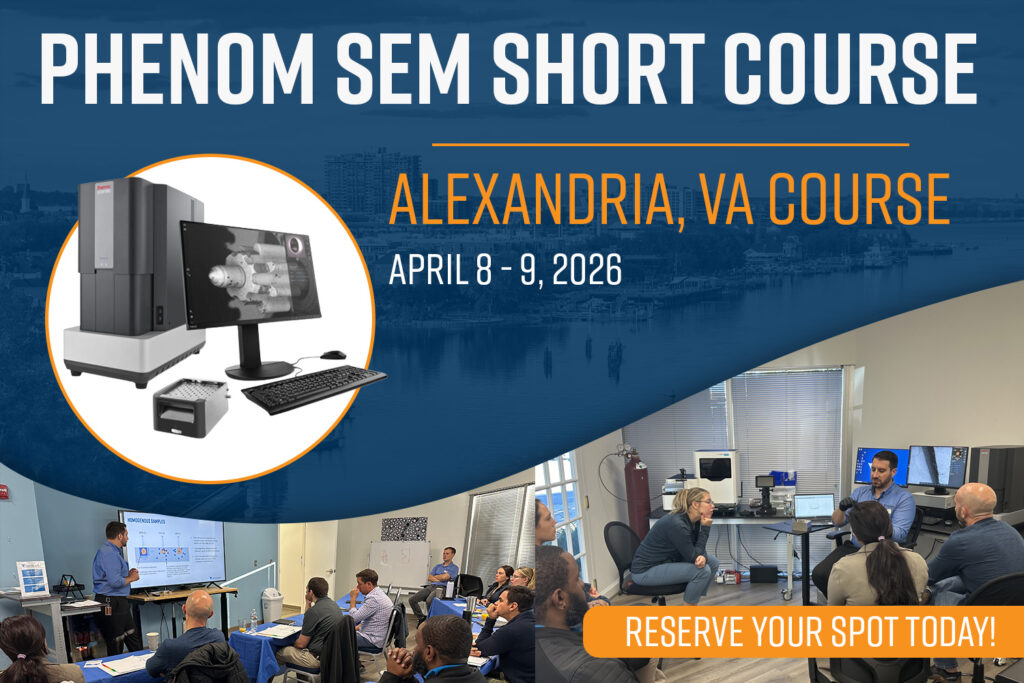
2-Day SEM Short Courses: Explore the microscopic world in our specialized 2-day Scanning Electron Microscopy (SEM) Short Course. Held in Alexandria, VA, this immersive program is designed for both experienced practitioners and newcomers, offering an in-depth exploration of both fundamental and advanced SEM techniques. Hosted at our state-of-the-art facilities, the course features hands-on sessions with […]
Broad Ion Beam vs. Focused Ion Beam Polishing: Choosing the Right Technique for Sample Preparation
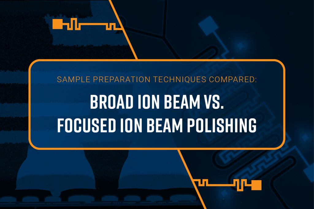
When preparing samples for electron microscopy, the choice of method directly impacts the clarity and reliability of the images. Imperfections such as roughness, contamination, or surface damage can obscure fine details and lead to misinterpreted data. Ion beam polishing, also known as ion beam milling, is an advanced sample preparation method that uses a directed […]
What is a Twin Screw Extruder? Types, Applications, and Benefits Explained
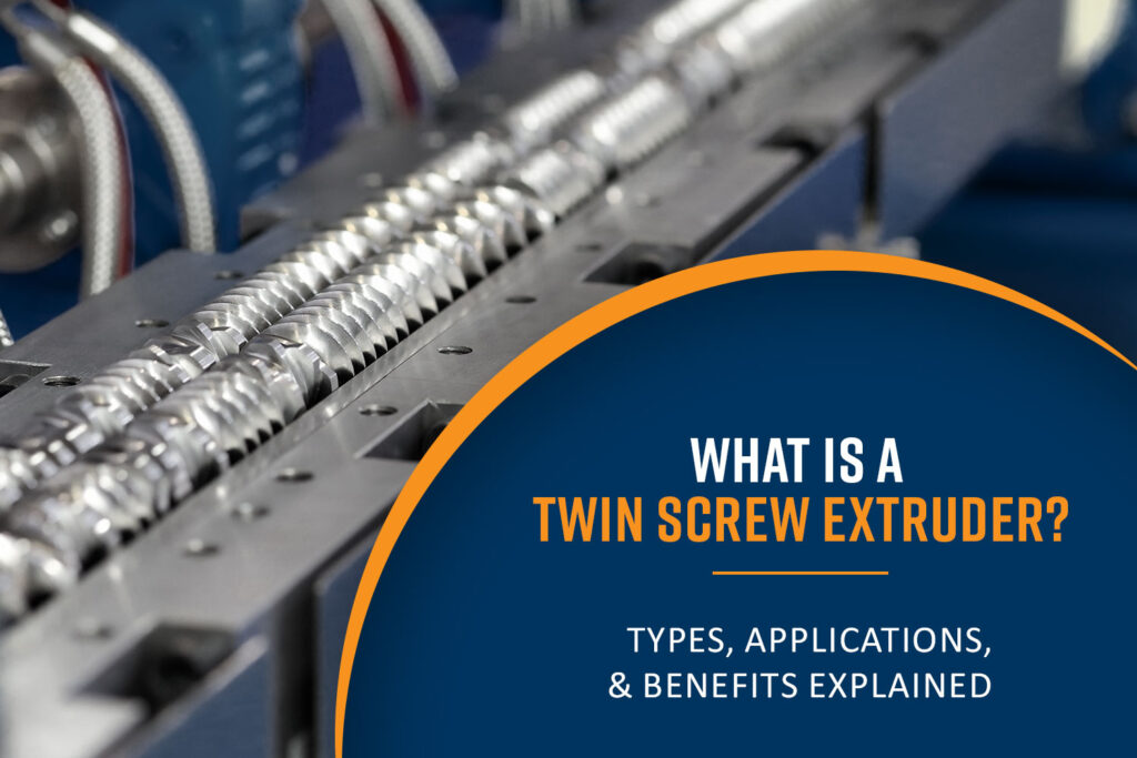
Twin screw extruders are among the most versatile processing equipment used in polymer compounding, pharmaceutical hot-melt extrusion, food production, and advanced materials research. They provide the precision and flexibility needed for complex formulations. Twin screw extruders offer superior mixing, enhanced process control, and facile scalability making them indispensable in industries where performance and consistency are […]
2-Day SEM Short Course | Phoenix, AZ | February 2026

2-Day SEM Short Course: Explore the microscopic world in our specialized 2-day Scanning Electron Microscopy (SEM) Short Course. Held in Phoenix, AZ, this immersive program is designed for both experienced practitioners and newcomers, offering an in-depth exploration of both fundamental and advanced SEM techniques. Hosted at our state-of-the-art facilities, the course features hands-on sessions with […]
ISTFA 2025 | November 17-19, 2025 | Pasadena, CA
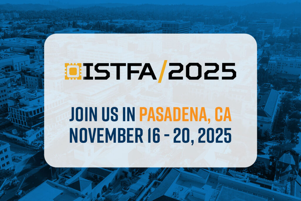
ISTFA 2025 Stop by and visit Nanoscience Instruments at booth #418 for the International Symposium for Testing and Failure Analysis (ISFTA) and discover how our class-leading microscopy solutions can elevate your material analysis! Get hands-on experience with the Phenom desktop SEM, featuring ChemiSEM technology that allows you to simultaneously visualize sample morphology and elemental distribution […]
Optical Microscopy vs SEM for Technical Cleanliness Analysis
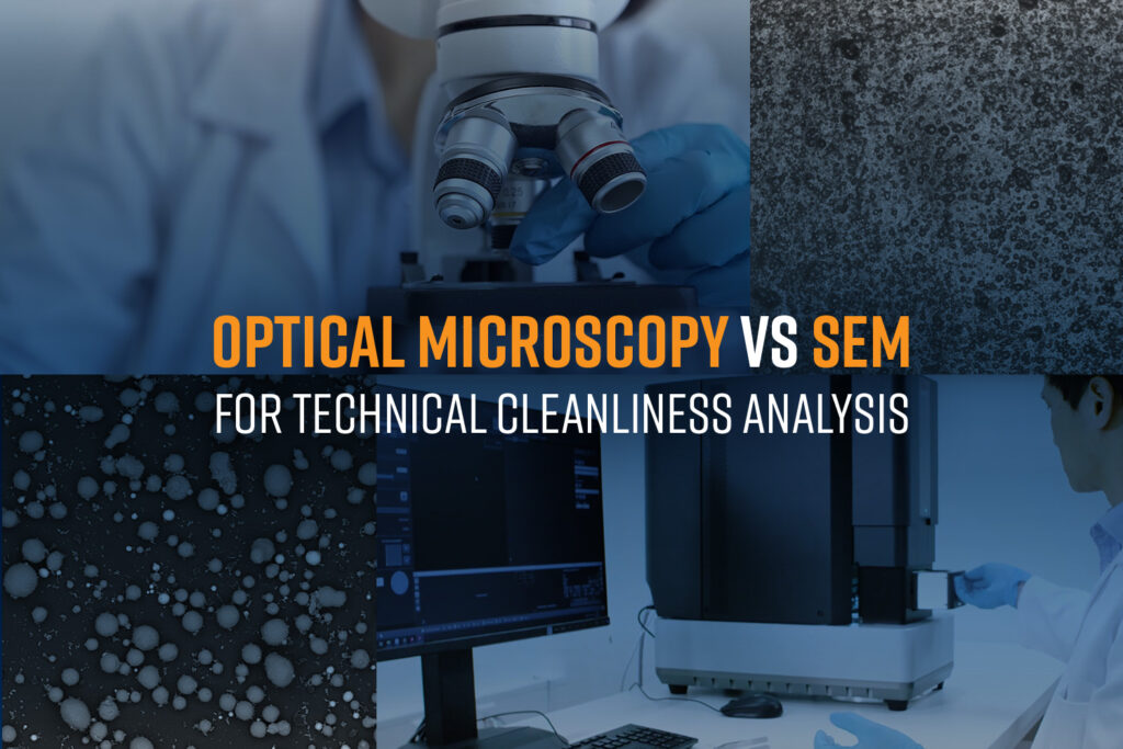
The performance of sensitive systems such as engines, hydraulics, electronics, and medical devices can be compromised in cases of particle contamination; this reduces product quality and introduces risks of failure. To prevent this, system components must meet standards of technical cleanliness (TC) to be accepted for use. Particulate quantity, size, and hardness are all considered […]
Choosing Between Optical and SEM Techniques for Particle Characterization
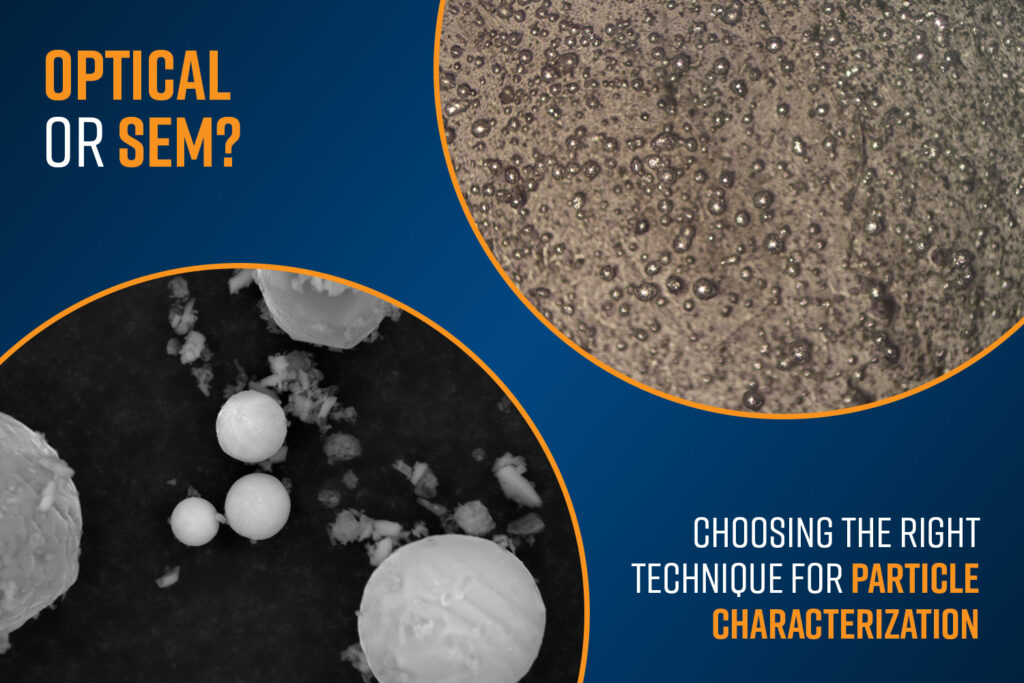
Particle analysis, which typically focuses on parameters such as size, shape, distribution, concentration, and composition, plays a critical role across a wide range of industries, from pharmaceuticals and biotechnology to advanced manufacturing and materials engineering., Two primary methods are commonly used to analyze particles: optical methods and scanning electron microscopy (SEM). While both aim to […]
The Battery Show 2025 | October 6-9, 2025 | Detroit, MI
Nanoscience Instruments provides solutions for battery development applications through cutting-edge instrumentation and analytical services. Visit our booth for live demonstrations of desktop SEM with automated workflows designed for structural and chemical analysis of battery materials, and learn about our surface characterization tools, battery cyclers & potentiostats, and process development and analytical services.