Electron microscopy is best known as a high-powered microscopy technique that utilizes a beam of electrons as a source of illumination. In an electron microscope, a focused electron beam interacts with the sample surface, leading to various beam-sample interactions. Each interaction generates a distinct signal that can be utilized to produce a high-resolution image.
Unlike light microscopy, electron microscopy can be used to acquire images at significantly higher magnifications to reveal an incredible amount of detail about the surface and internal structure of a sample. Today, electron microscopes are used for a wide variety of applications from quality control to visualizing the atomic structures of next-generation materials.
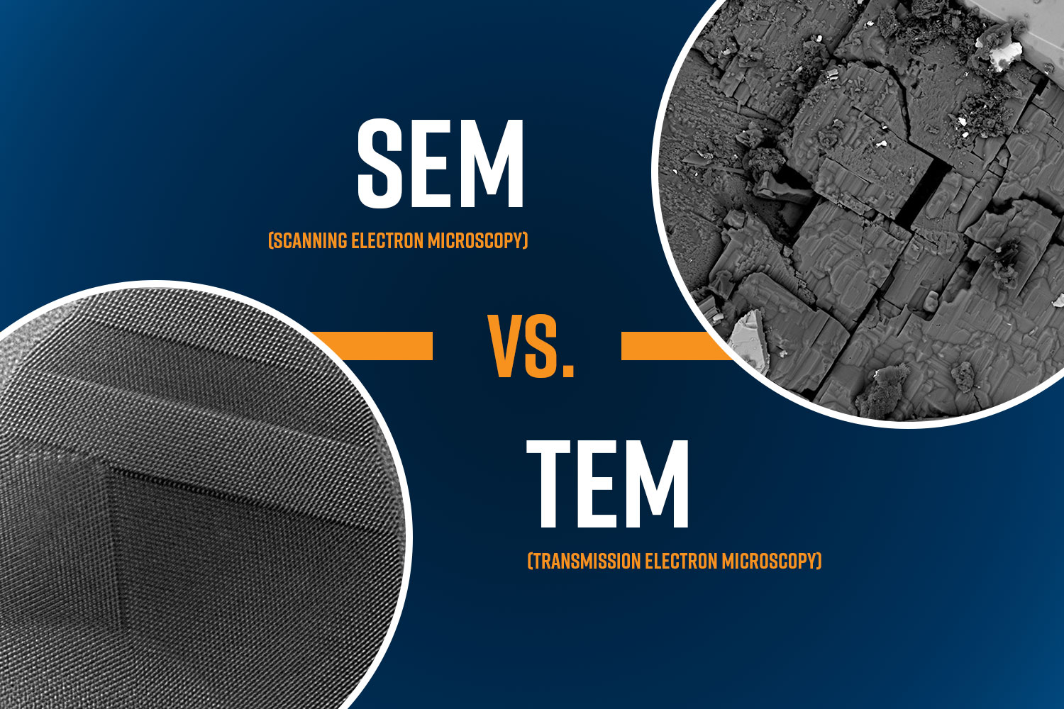
SEM vs. TEM
Scanning electron microscopy (SEM) and transmission electron microscopy (TEM) are the two most common forms of electron microscopy. While both techniques share the same fundamental principles, there are several distinct differences in their instrumentation and what signals are analyzed. In an SEM, the secondary electron (SE) and backscattered electrons (BSE) are used to acquire images of a sample’s surface whereas in a TEM, the transmitted electrons are detected to produce a projection-image through a sample’s interior. In this article, we’ll dive into these two popular electron microscopy techniques and provide a brief comparison between their key operational and practical differences.
What do all electron microscopes have in common?
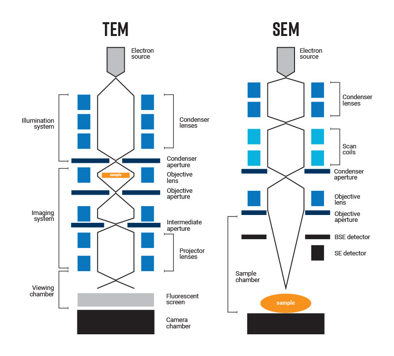
To make a meaningful comparison between SEM and TEM, it’s important to note what all electron microscopes have in common. The “column” of all electron microscopes contains a series of components that are responsible for core functions. These include:
- The electron source – produces the electron beam.
- Condenser lenses – directs the beam onto the sample.
- Objective lens – containing the most important electromagnetic lens in the column, is responsible for forming an image of the transmitted electrons (TEM) or for forming the final focused probe that is scanned across the sample surface (SEM).
- Sample chamber – holds the sample and determines the size of the sample that can be analyzed.
- Detectors – collect signals to produce images.

Scanning Electron Microscopy (SEM) Basics
An SEM uses a focused electron beam to scan the surface of a sample and the signals generated are collected at each point to build up a magnified image in a pixel-by-pixel fashion. Scanning coils, located below the condenser lenses are used to precisely direct the beam across the sample’s surface in the X-Y plane. Depending on magnification, which can reach up to 2 million times, the beam will scan over a field of view ranging from a few micrometers up to several millimeters. Bulk samples can be directly analyzed without further preparation if they fit within the sample chamber.
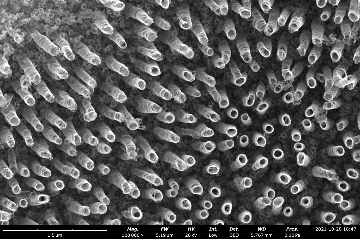
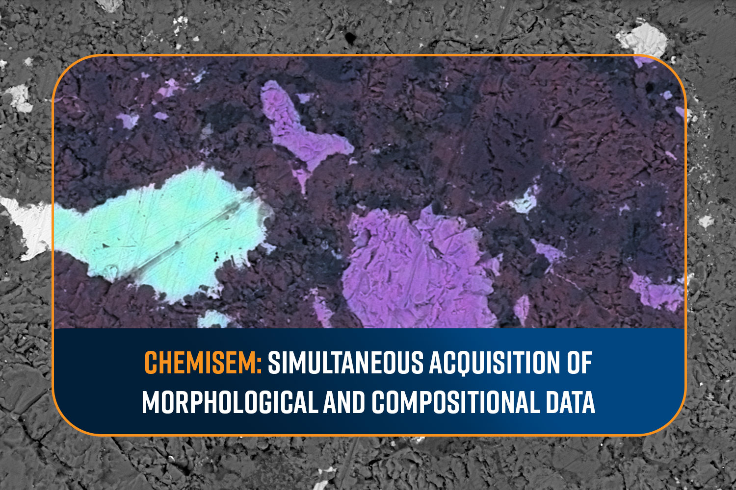
The primary signals used for image generation in an SEM are the backscattered electrons (BSEs) and secondary electrons (SEs). Each of these signals is generated when the electron beam interacts with the subsurface of the sample. The SEs come from a distinctly shallower region than the BSEs. Importantly, this means that an SEM can produce images of a sample’s surface, allowing scientists to visualize surface morphology, surface composition, and surface topography. Depending on the flatness of the sample, SEM images can have a 3D appearance.
Typical accelerating voltages for SEM range from 1 keV up to 30 keV. Lower accelerating voltages provide a gentler beam that can be useful when imaging beam-sensitive and insulating samples. A higher accelerating voltage allows for improved spatial resolution. For example, a field emission SEM using an SE detector can routinely resolve features <2 nm apart.
Transmission Electron Microscopy (TEM) Basics
A TEM produces a magnified image of a sample by illuminating it with a broad beam of electrons and detecting the transmitted electrons in a single frame. Unlike SEM, no scanning coils are needed to raster the beam across the sample. Instead, a broad beam (often referred to as “parallel illumination” to describe its plane-wave nature) is formed by the illumination system. The objective lens in a TEM plays a crucial role in forming a high-resolution image from the transmitted electrons that emerge from the sample’s exit surface.
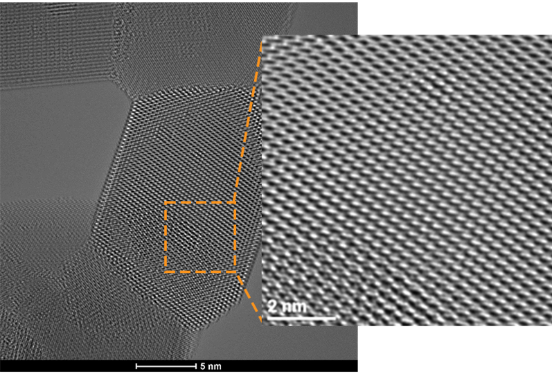
The magnification of a TEM image can reach beyond 50 million times, allowing for crystalline atomic structures to be directly visualized. Samples need to be extremely thin to be compatible with TEM, usually less than 100 nm, which allows for the beam to transmit through the sample.
The transmitted electrons that are analyzed in a TEM can be separated into different categories including the direct beam and diffracted beams. Intermediate lenses and apertures located below the sample can be adjusted to form images from specific diffracted beams which help scientists understand more about a sample’s crystalline structure, as well as its defects. The projector lenses are used to control magnification and project the transmitted electrons onto a fluorescent viewing screen, or a digital camera located at the bottom of the column.
Accelerating voltages in TEM typically range from 30 kV up to 300 kV, which is considerably higher than what is used in SEM instruments because it allows for even higher-resolution images to be generated. An aberration-corrected TEM can routinely achieve spatial resolution of less than <1 Å, which allows it to produce stunningly detailed images of the smallest structures in matter, such as the individual atomic arrangements within nanoparticles.
Summarizing the key differences between SEM and TEM:
| SEM | TEM | |
| Signals analyzed | Backscattered electrons, secondary electrons | Transmitted electrons |
| Image formation mechanism | The beam is scanned across the sample surface and signals are collected in a pixel-by-pixel fashion | Static beam illuminates the sample and a projection image of the transmitted beam is acquired in a single frame |
| Sample thickness | Any (limited by sample chamber) | <100 nm for most materials |
| Accelerating voltage | ~1-30 kV | ~30-300 kV |
| Type of information in the image | Surface compositional contrast, surface morphology, surface topography (can have 3D appearance) | Phase or diffraction contrast image through sample’s surface and internal structure (2D appearance) |
| Max magnification | Up to 1-2 million times | 50 million times or more |
| Typical field of view | A few µm to several mm’s | A few nm’s up to several µm |
| Spatial resolution | ~1-2 nm | <1 Å |
| Size of instrument | Smaller, desktop models and floor model options | Larger and taller, takes up entire room |
| Cost | Less expensive | More expensive |
| Time-to-image | Fast | Slow |
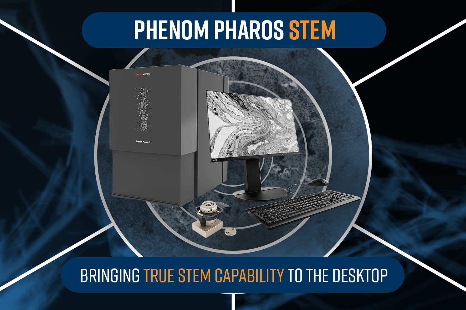
What about STEM?
STEM, which stands for scanning transmission electron microscopy, can be thought of as a hybrid between SEM and TEM. In a STEM, a thin sample is scanned with a focused electron beam (like an SEM) and the transmitted electrons are detected (like in TEM) at each point to acquire a high-resolution image of the internal structure of the sample.
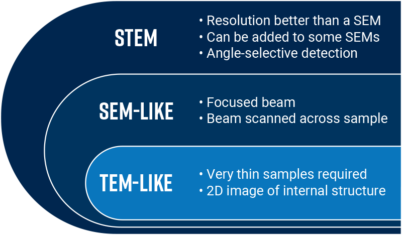
The technique presents some unique advantages, namely its ability to achieve a higher resolution than SEM (e.g., <1 nm) and the opportunity to analyze signals based on scattering angle, which provides the flexibility to produce bright-field (phase contrast) and dark-field (compositional contrast) images.
Because of the similarities between STEM and SEM, some SEM instruments can be operated in STEM mode (also known as “STEM-in-SEM”). Typically, this added functionality would be reserved for a field-emission SEM because its ultra-bright electron source supports higher resolution and better signal-to-noise which becomes critical when operating in STEM mode. All that is needed is the addition of a STEM-in-SEM detector or a STEM conversion sample holder.
Other key differences between SEM and TEM
Beyond the major operational and instrumentation variations, there are a few other key differences between SEM and TEM that are worth mentioning:
Training and support
SEMs are comparatively simpler instruments than TEMs. Training is much easier and they present fewer opportunities for problems to arise. An SEM will experience very little scheduled downtime aside from regular electron source changes. It is feasible to train a large group of users and not worry about the instrument being unavailable, which can make it a very valuable tool in an industrial or R&D setting.
On the other hand, for a TEM to consistently deliver quality high-resolution images, skilled operators and the ability to support more frequent troubleshooting and potentially expensive repairs is a requirement. In general, the user base for a TEM will be limited to a group of highly trained individuals.
Automation
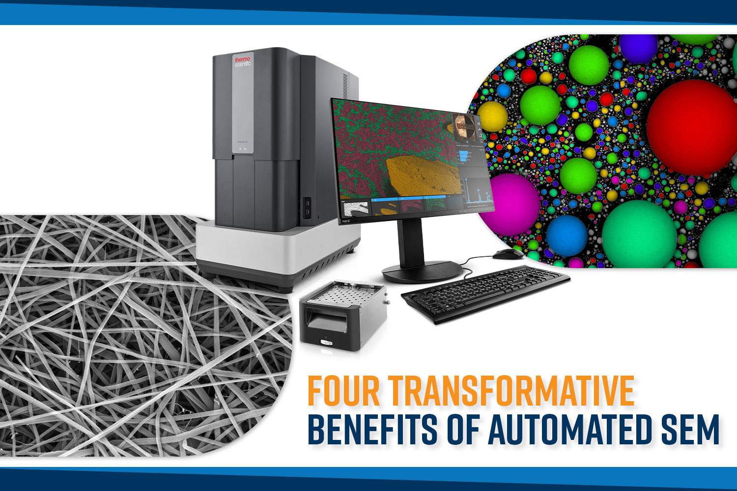
For well-defined workflows, some SEM modes provide the opportunity for automating data collection and analysis. A fully automated SEM can handle everything from auto alignment to selecting areas of interest, acquiring high-quality images, analyzing the data, and generating a summary report of the results. Some common examples of where automated SEM is valuable are for monitoring technical cleanliness of manufactured parts, trace evidence analysis (e.g., gunshot residue), steel inclusion analysis, and quality control of battery materials. Depending on the specific goals and resources within an organization, it might make more sense to purchase an off-the-shelf solution or to build a customized routine.
In regard to TEM, there are a growing number of automation solutions that allow microscopists to more efficiently collect data for advanced experiments such as in situ TEM. However, fully automated routines on-par with what SEMs are currently capable of are not as readily available.
Sample Preparation
SEMs have a larger sample chamber than TEM and therefore can handle a bulk sample that is up to a few centimeters squared in size. Many samples can be analyzed without further preparation, making it a convenient non-destructive technique to have on hand. Analyzing the same sample in a TEM can require extensive preparation. Bulk materials need to be thinned to less than around 100 nm to be electron-transparent and preparing such a thin specimen requires specialized tools for thinning and final cleaning.
Conclusion
Electron microscopy allows scientists to visualize materials at extremely small length scales. Between SEM and TEM, choosing the right technique for your application ultimately comes down to what information you are trying to learn about a sample. In some cases, having the ability to do both will provide the complimentary analysis needed. Here are some key takeaways to keep in mind if you are in the process of acquiring new electron microscopy instrumentation:
- What types of structures are you analyzing and what resolution is needed?
- Are you trying to learn about the surface or internal structure, or both?
- Is your workflow well-defined and does it lend itself to automation?
- What types of facilities do you have available and is space a limitation?
To explore more about selecting the right SEM for you, check out our articles on SEM cost, what factors to consider when purchasing an SEM, floor models vs desktop SEM models, and how to choose a desktop SEM model to fit your needs.