Table of Contents

What is scanning transmission electron microscopy (STEM)?
Scanning transmission electron microscopy (STEM) is an advanced imaging technique that is used to visualize the structure and composition of materials at nanometer to sub-atomic length scales. It provides high-resolution images and spectroscopic data by scanning a focused electron beam across a very thin sample and collecting various signals in parallel. The most common signals acquired in STEM are bright field (BF), annular dark field (ADF), and high-angle annular dark field (HAADF) images. The technique is commonly paired with energy-dispersive X-ray spectroscopy (EDS) and electron energy-loss spectroscopy (EELS) to provide correlative spectral maps of elemental composition and electronic structure.
Materials prepared for STEM need to be electron-transparent, meaning they allow electrons to transmit through the sample with minimal scattering. This property enables a high number of transmitted electrons to be collected by the different detectors, thereby improving signal-to-noise. Typical STEM samples, including tissue sections, lamella, and nanoparticles on the order of 100 nm thickness or less, meet the criteria for electron transparency.
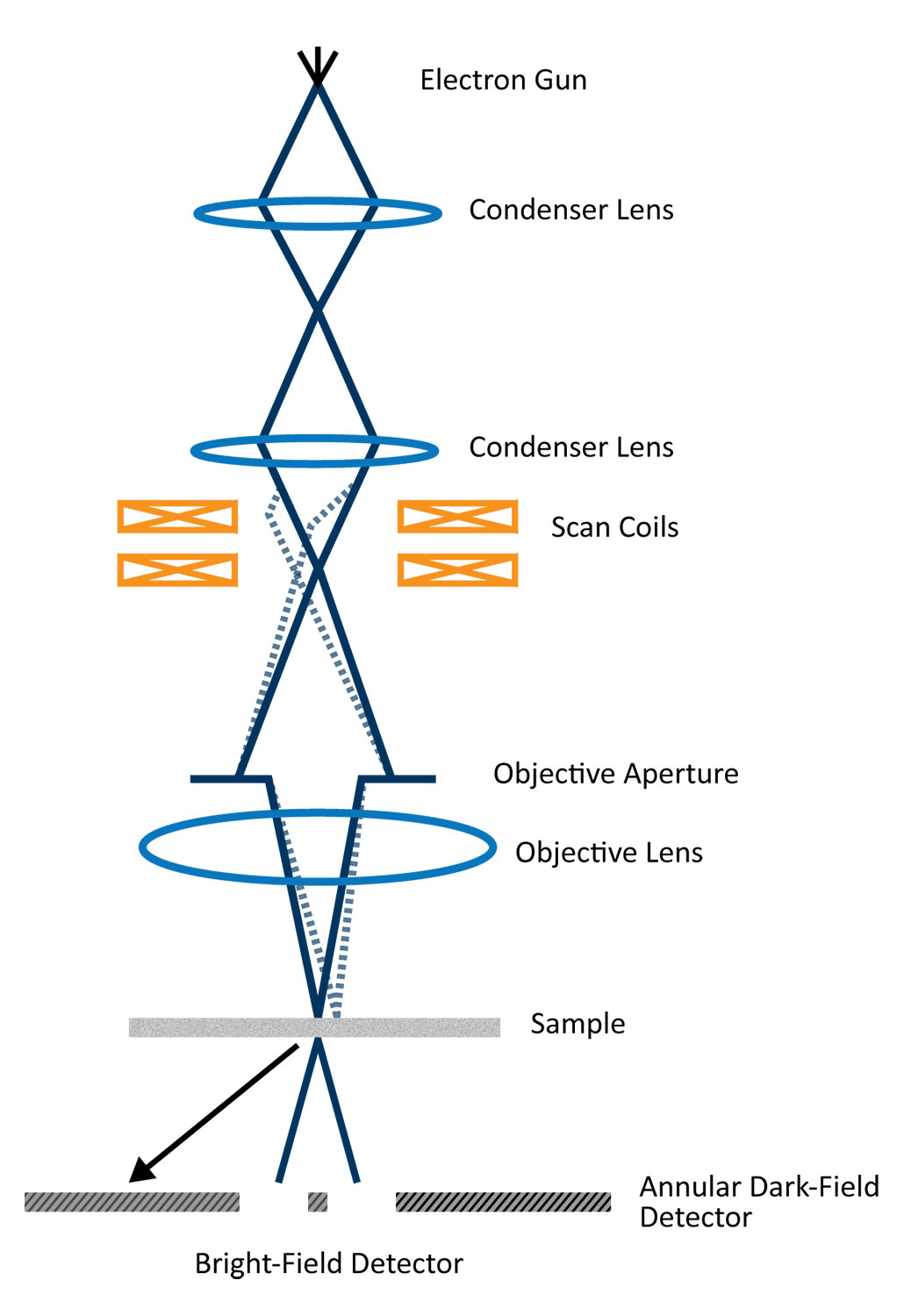
STEM was originally invented on the principle that its configuration separates the probe-forming optics from the detector optics, allowing for more flexibility and the ability to collect multiple signals at the same time. Innovations in electron gun technology — namely the invention of the cold field-emission gun (C-FEG) — have made modern STEM possible [1]. The superior coherence of electrons emitted from a C-FEG allows for the condenser lens system to focus the incident electrons on the sample to an extremely small point. With aberration correction, the STEM probe can be made smaller than the interatomic distances (e.g., 100 pm), allowing for directly interpretable images when using HAADF imaging [2]. With some modifications, most conventional transmission electron microscopes (TEMs) can be used for STEM imaging by equipping them with additional scanning coils and tuning the condenser lens system to create convergent illumination. However, dedicated STEMs are also common for their high stability since lens currents are kept constant [3].

What is STEM used for?
STEM is widely leveraged in the domains of materials science and biology for its capabilities to provide a multitude of localized signals regarding a sample’s physical structure, electronic structure, and composition. Here are but a few examples of STEM applications [4]:
Ceramic grain boundaries: In the study of grain boundaries in ceramics, the grain boundary character significantly influences bulk materials properties such as ionic conductivity. STEM is uniquely suited to not only identifying a grain boundary’s atomic structure, but it is also possible to detect individual dopant sites. Unlike TEM, there are no contrast reversals in HAADF images which makes determining complex atomic structures less challenging.
Semiconductor interfaces: STEM is a major analytical technique used in the semiconductor development process as it can reveal the atomic structure of interfaces between semiconductors, metals, and dielectrics within transistor gate structures. HAADF imaging and EELS can be used together to study the atomic and electronic structure of high-k dielectric/semiconductor interfaces, as well as other types of interfaces. This allows for a fundamental understanding of how structural defects impact the functioning of semiconductor devices.
Heterogeneous catalysis: The goal of heterogenous catalysis is to speed up the rate of chemical reactions. Therefore, catalysts are often composed of supported nanoparticles wherein the exposed surfaces are tailored to maximize catalytic activity. The exact effect of the catalyst depends upon the atomic and electronic structure at the surface, which in turn influences the way in which molecules adsorb, desorb, and participate in chemical reactions. STEM is well suited to study these materials because it has the resolution to see the relevant structures involved in potential catalytic reactions. In situ STEM is often used to perform nanocharacterization of catalysts under near-reaction conditions by exposing them to heat and reactive gases and observing changes via STEM imaging.
Amorphous materials: A form of STEM, called fluctuation electron microscopy (FEM), is used to study medium-range order (MRO) in amorphous and disordered materials. Materials that lack long-range periodicity (e.g., polymers, glass) can exhibit periodicity on shorter length scales, such as nearest-neighbor distances between neighboring atoms, sometimes at preferred scattering angles. In FEM-STEM, a series of nanodiffraction patterns are acquired in STEM mode and fluctuations in the diffracted intensity are measured to yield information on MRO.
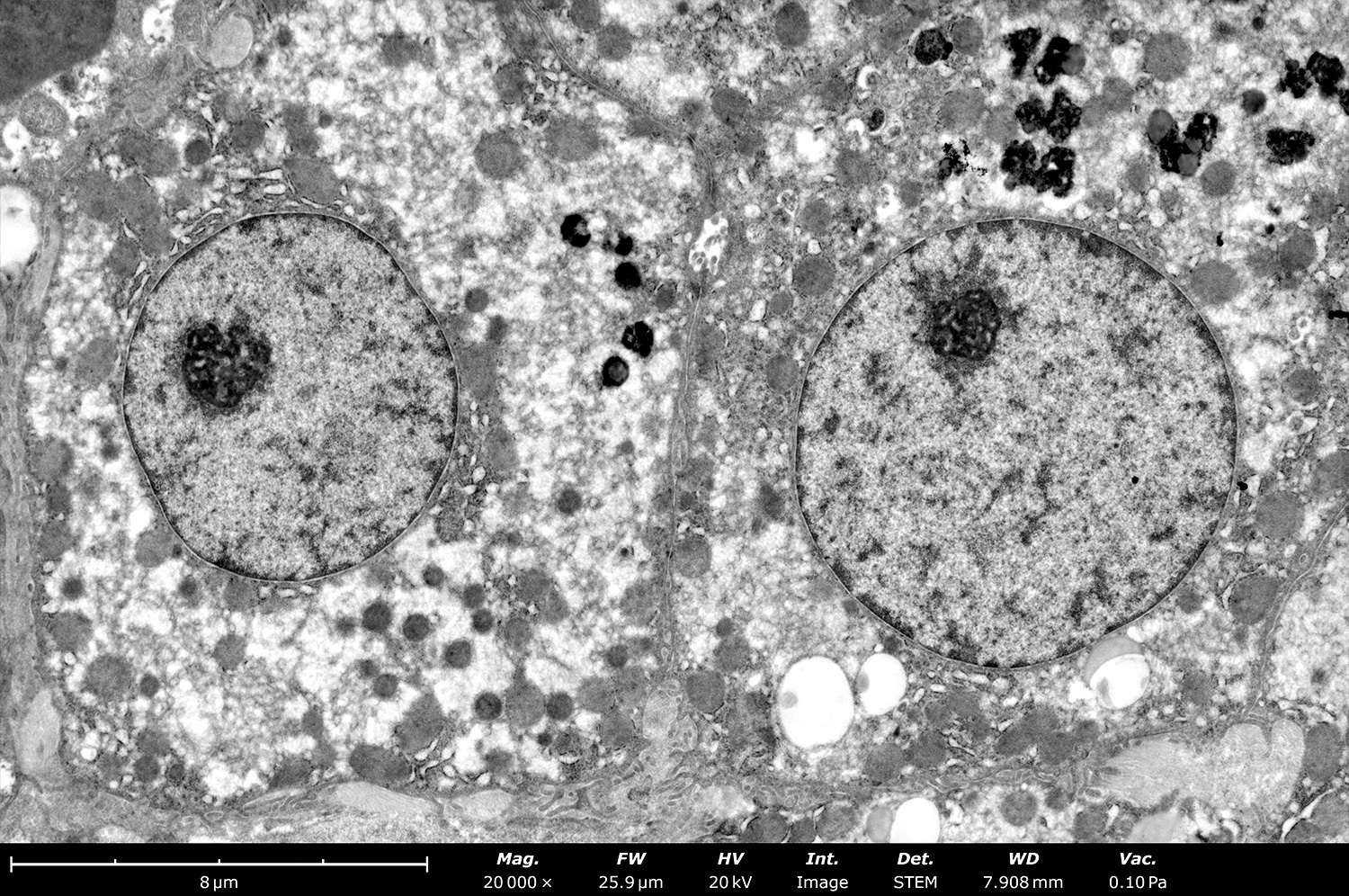
Biological sciences: There are several ways in which STEM is applied to biological materials. Mass determination of macromolecular assemblies can be precisely measured with HAADF imaging since the HAADF signal is directly proportional to mass-thickness [5]. It has been most widely used for filamentous structures like DNA. Both the ADF and HAADF signals can also be used to visualize specific proteins that are labeled with heavy atoms. STEM-EELS has been used to map the localized bonding throughout sectioned cells. Finally, electron tomography acquired in the STEM can yield 3D reconstruction of cells and cell sections up to one micrometer in thickness.
How is STEM different from TEM?
Convergent beam illumination
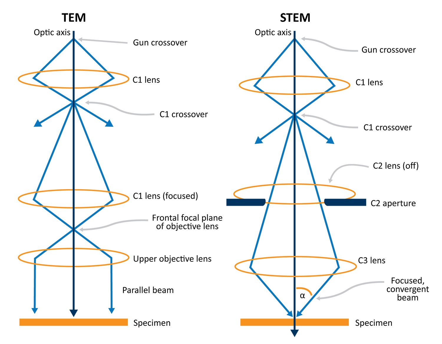
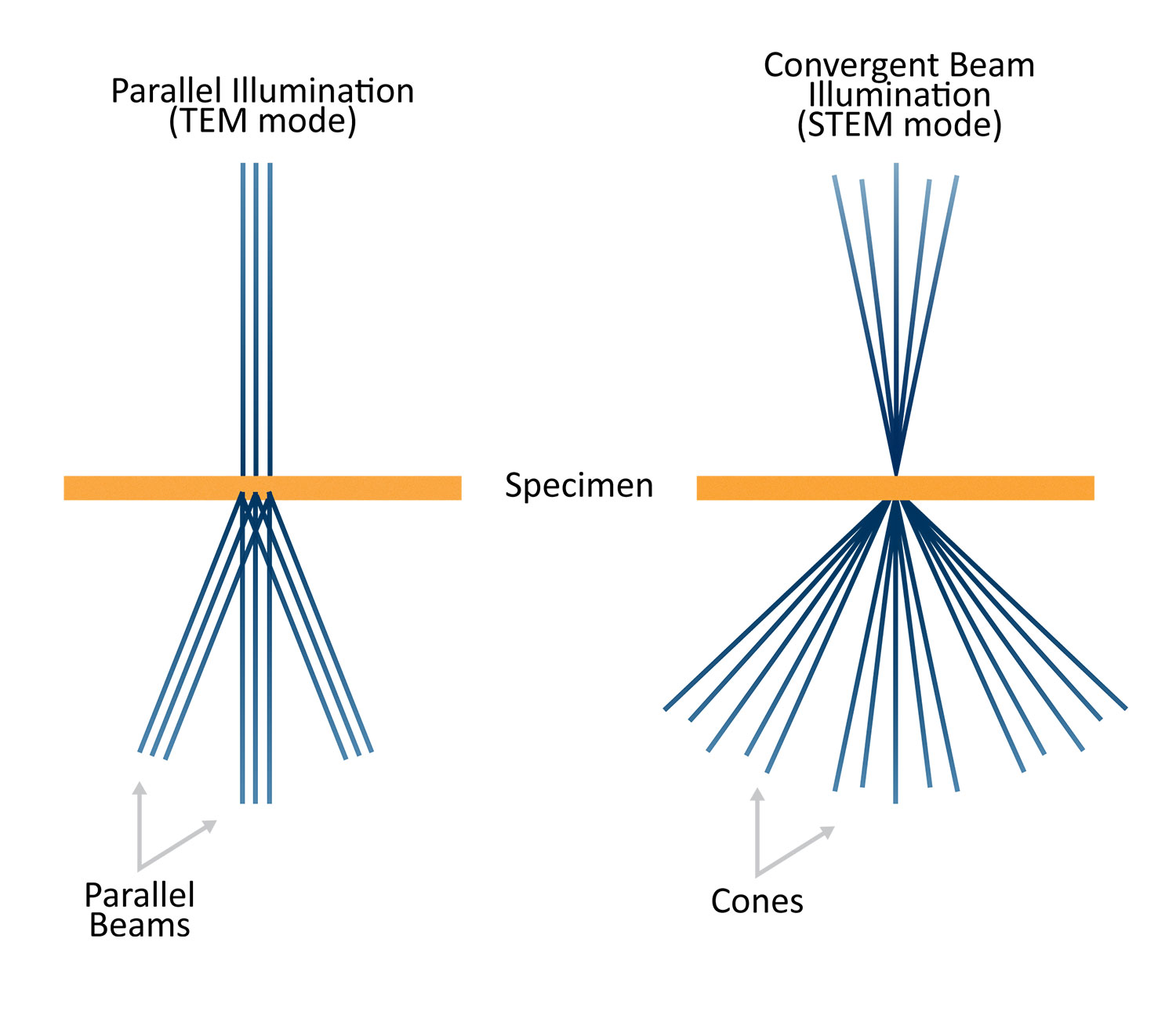
The main difference between STEM and TEM is the beam formation optics which result in different beam convergence angles (α) at the specimen surface. In TEM mode, a parallel beam (α ~ 0°) is desired. The first (C1) and second (C2) condenser lenses are excited such that an image of the gun crossover is formed on the front focal plane of the objective lens upper polepiece (C3). This allows for a broad, parallel beam to be projected onto the sample. For STEM, a large value of α is needed in order to form a small, localized probe on the sample surface. By shutting off the C2 lens, an image of the gun crossover is formed far away from C3. This allows for a large demagnification of the crossover to be formed at the sample surface and a C2 aperture is inserted to precisely define α and minimize aberrations.
Magnification not by lenses
In STEM, images are built up pixel by pixel by scanning the beam across a fixed field of view using scan coils. Therefore, the magnification is controlled by the scanned area. If the scanned area is 1 mm x 1 mm on the sample and is displayed on a computer screen at 100 mm x 100 mm, then the magnification is 100x. Magnification can reach up to 107x in STEM [6]. The detector and the digital image recording software allow the number of pixels within the scanned area to be varied and can range from 256×256 pixels up to 2048×2048 pixels, depending on the detector configuration. Scanning smaller areas corresponds to an increased magnification whereas increased pixel densities increase the apparent resolution. On the other hand, a fixed area of the sample is illuminated by a parallel beam in TEM. Post-specimen intermediate lenses magnify the transmitted signal onto detectors to define what area of the sample is used to generate an image, thereby defining the magnification. Similar to STEM mode, pixel density impacts the apparent resolution in a TEM image in combination with magnification.
Convergent beam electron diffraction (CBED) pattern
As the probe scans across the sample, a stationary convergent beam electron diffraction pattern (CBED) forms in the objective lens’s back focal plane. The range of incident angles (determined by α) becomes scattered according to the Bragg scattering angles into cones which cause the diffraction disks to form. The symmetry and arrangement of these disks convey information regarding the crystalline structure and symmetry within the specimen. The diffraction pattern in TEM will have the same symmetry but will feature well-defined spots due to the negligible range in α. The main difference between the direct beam in TEM vs STEM is that the central disk in the CBED pattern can contain phase-contrast information. This is because non-parallel incident beams may be Bragg diffracted into a parallel condition and subsequently interfere constructively or destructively with the undiffracted beams.
STEM Detectors
The electrons contributing to STEM images can be finely controlled by varying the camera length and inserting various detectors. STEM detectors function the same way objective apertures do in TEM.
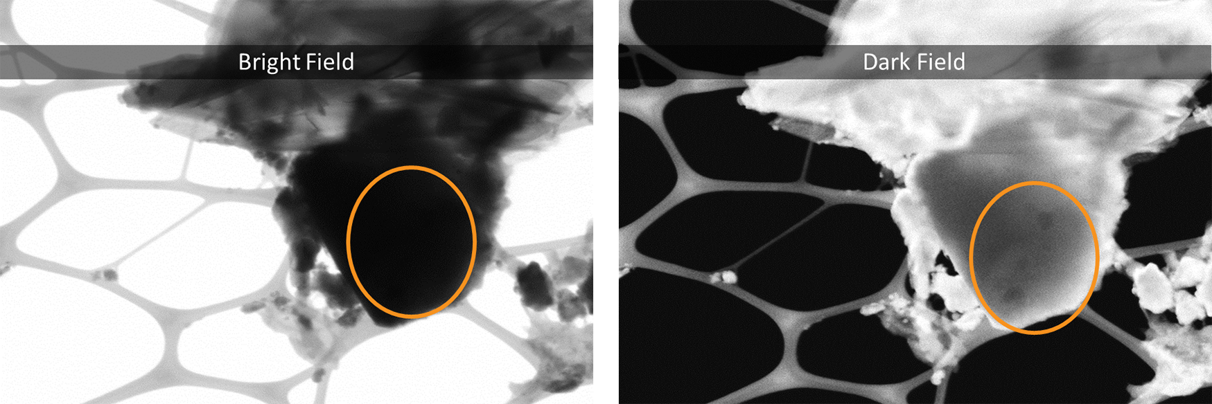
Bright-field (BF): The BF detector sits on-axis and collects electrons contributing to the central disk in the CBED pattern. A typical acceptance angle for the BF detector is half of α. BF-STEM images are analogous to phase-contrast images in TEM and can provide high-resolution information with enhanced contrast of light elements.
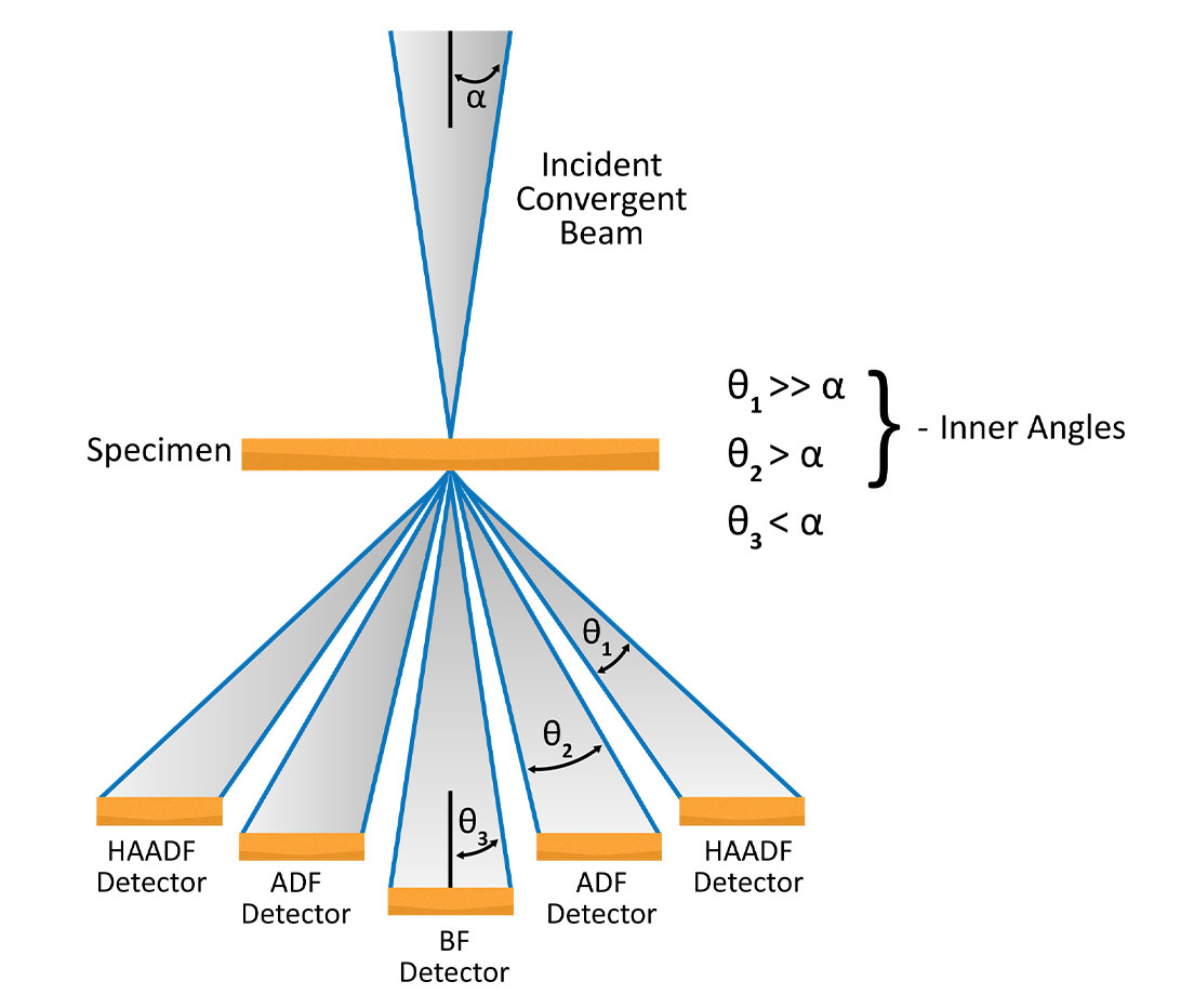
Figure 4. Schematic diagram of STEM detector set up.6
Annular dark field (ADF): ADF images are acquired using a ring-shaped detector that surrounds the BF detector so that a large portion of the Bragg-diffracted electrons are collected. These images are complementary to the BF-STEM images in terms of contrast. Compared to DF-TEM images, which use an objective aperture to only include one diffracted beam into the electrons that make up an image, ADF-STEM imaging provides improved signal collection efficiency. The annular detector also allows for the central transmitted beam to be collected in an electron energy-loss spectroscopy (EELS) detector.
High-angle annular dark field (HAADF): HAADF imaging is similar to ADF imaging except only electrons scattered to a very high angle are included. As a result, the signal is dominated by incoherently (Rutherford) scattered electrons which originate from interactions between the incident electrons and the nuclei of atoms within the sample. Therefore, HAADF image contrast is sensitive to atomic number and can be used to generate atomic-resolution images wherein heavy atoms appear brightest. One drawback of HAADF imaging is that the contrast depends upon Z2, where Z is the atomic number. For example, in metal oxides, only the metal cations are visible and the oxygen columns are not usually visible.
What is STEM-in-SEM?
Another variation of the technique is STEM-in-SEM, where STEM imaging is conducted in a scanning electron microscope (SEM) [7]. STEM-in-SEM combines two fundamental concepts. Firstly, SEM instruments use a focused electron beam to scan a sample surface. Second, images are acquired by collecting the transmitted electrons that emit beneath the sample as in the case with a STEM or TEM instrument. As a result, an electron transparent sample (<100 nm) must be used in a place of bulk sample to collect a meaningful STEM-in-SEM analysis.
The main motivation for developing this technique is due to the resolution limitation of SEM [8]. In SEM, the resolution is limited by the relatively large volume of interaction, which extends into the subsurface region of bulk samples. By making the sample electron-transparent, the volume of interaction is reduced so that the resolution is limited by the probe size (about 1 nm with a FEG source). By collecting transmitted electrons, there is also the option to discriminate based on the scattering angle which forms the basis of bright field (BF), annular dark field (ADF), and high-angle annular dark field (HAADF) signals.
STEM-in-SEM Instrumentation
Upgrading a SEM to allow for STEM-in-SEM is relatively straightforward. A STEM sample holder and either a STEM detector or signal conversion piece are required [7]. Depending on the microscope manufacturer, there will be various configurations available that utilize one or both options. It is recommended that the SEM already have a field-emission gun (FEG) as this provides the smallest probe size compared to thermionic emitters such as those based on tungsten or cerium/lanthanum hexaboride. The high brightness beam made possible by a FEG system also increases the total number of transmitted electrons needed for most STEM detectors to produce images with acceptable signal-to-noise ratios.
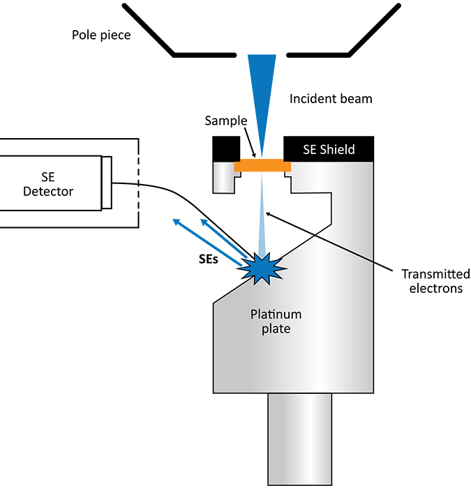
STEM conversion sample holder
A STEM conversion sample holder is the simplest configuration for enabling STEM-in-SEM. It holds an electron-transparent sample in the optical axis allowing transmitted electrons to strike a platinum plate below the sample, generating a new signal of secondary electrons [7]. These electrons are directed to the secondary electron detector (SED) based on the angle of the plate with respect to the detector. STEM images are built up pixel-by-pixel as the beam scans the sample. A cylindrical sleeve is placed close to the pole piece above the sample to block secondary electrons originating from the sample from reaching the detector. As a result, the conversion holder cannot be used with bulk samples for SED imaging. Another consequence of this apparatus is that only forward scattered, or the BF signal, can be reliably collected. This pseudo-transmission signal intensity is overall quite weak and very sensitive to the positioning of the plate, meaning that careful alignment must take place each time the conversion holder is used.
STEM-in-SEM detectors
Solid-state STEM detectors allow the transmitted electrons to be directly detected. Advanced STEM-in-SEM detectors utilize segmented sensors that allow for angular selectivity and the independent acquisition of BF, ADF, or HAADF images. Each signal provides complimentary information about the sample allowing a more comprehensive analysis of the sample. Other detectors may use physical masks to block electrons from specific scattering angles from reaching the detector. The apparatus that the detector is contained within will depend upon the configuration of the SEM as well as what level of alignment is needed, if any, to operate the detector once it is installed.
Comparison of STEM-in-SEM instrumentation
| STEM Conversion Holder | STEM-in-SEM | |||
| Mechanism | Indirect signal detection with SED and platinum “reflector” plate | Direct signal detection with dedicated solid-state detector (may be segmented or utilize physical masks) | ||
| STEM Modes | BF only | BF, ADF, HAADF | ||
| Costs | Low-cost SEM accessory | Moderate upfront cost to add to SEM | ||
| Requirements | Existing SEM with SED | Existing compatible SEM (FE source recommended) | ||
STEM-in-SEM Applications
Although STEM-in-SEM does not compete with the spatial resolution of conventional STEM (<0.1-nm with aberration correction) due to the lower accelerating voltages used and ease of use, it has gained popularity for applications that do not demand the highest resolutions while freeing up valuable time on aberration-corrected TEM and STEM instruments.
Pathology
The resolution and contrast provided by STEM-in-SEM is sufficient to see organelles within metal-stained cell cross-sections. While dedicated TEMs have historically been used for this purpose, they are more challenging for users to learn and operate. With the sample preparation used for both techniques being the same, STEM-in-SEM provides advantages in sample throughput, ease of use, and the ability to image at much lower accelerating voltages to prevent sample degradation.
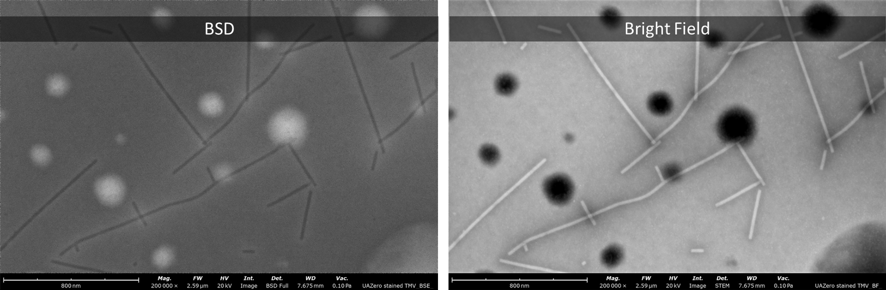
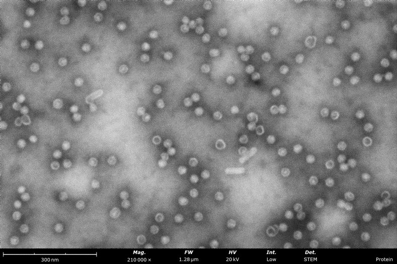
Microbiology
STEM-in-SEM provides utility in microbiological studies that use negative staining for electron microscopy imaging. STEM imaging provides much sharper images than SEM images acquired with a backscattered electron detector (BSD). For researchers that study viruses or bacteria by monitoring particles sizes and shape, this tool provides far superior imaging to traditional SEM and a faster workflow than dedicated S/TEMs.
Grid screening for Cryo-EM
Structural biology research based on electron imaging demands the extremely high resolution only aberration-corrected TEMs offer. For labs working on single analysis (SPA), STEM-in-SEM can expedite sample preparation workflows with an easy-to-use sample screening tool. In many cases, STEM-in-SEM images are sufficient to determine if the sample is worth the time and cost of performing TEM imaging.
Nanostructured materials
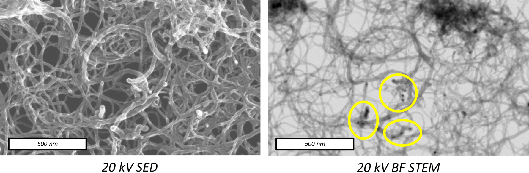
For nanoparticle samples, STEM-in-SEM provides far better resolution and detail than SEM imaging and can be a great substitute for the use of dedicated TEM/STEMs in applications that do not demand atomic resolution. For example, STEM-in-SEM has been widely used for the study of carbon nanotubes because the lower accelerating voltages allow for sample damage to be minimized [9]. It can also be used to characterize hierarchically structured nanomaterials, such as those used in heterogeneous catalysis including core-shell structures and catalyst-decorated supports.
What is 4D-STEM?
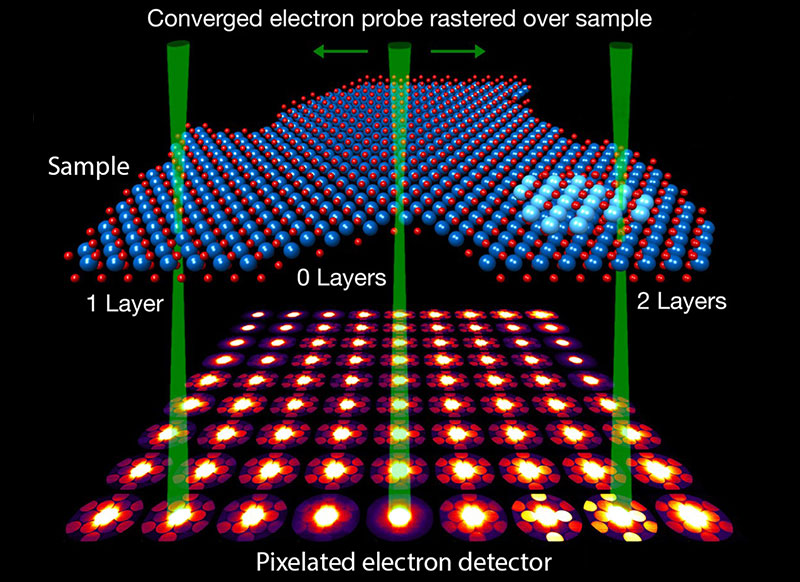
Four-dimensional (4D) STEM refers to recording the entire CBED pattern such that every point within the 2D scanned area (in real space) corresponds to a 2D CBED pattern (in reciprocal space) [10]. This has expanded the utility of STEM to allow scientists to explore even more aspects of nanomaterials, such as orientation and strain mapping, differential phase contrast, ptychography, and more. 4D-STEM is ideal for studying beam-sensitive materials because, in only one scan, the electron dose can be precisely set while a multitude of datasets can be mined from the 4D data cube [11].
Developments in detector technology have enabled 4D-STEM to become a reality. Conventional STEM detectors only record a single value, namely intensity (within a fixed angular range). On the other hand, TEM imaging cameras that are based on a charge-coupled device (CCD) architecture have relatively slow readout speeds and lower dynamic range. This limits their ability to keep up with the STEM scan coils (which set pixel dwell times on microsecond to millisecond time scales) and distinguish intensity differences between the central BF disk and high-angle scattered electrons.
Hybrid pixel detectors are a relatively new form of electron detectors that are composed of an array of semiconductor sensors that are individually bump-bonded to an application-specific integrated circuit (ASIC). They can be optimized for 4D-STEM experiments by having electron-counting circuits, which allows them to have single-electron sensitivity, high dynamic range, and fast readout speeds. They can also be configured for frame-based or event-driven readouts. Traditional frame-based detectors capture data from every pixel, even if some have zero electron counts, resulting in a complete array of intensity values within a single frame. In contrast, event-driven detection selectively reads out pixels that actually receive electrons. This distinction becomes especially significant when dealing with sparse data situations, greatly enhancing the speed and efficiency of data management for the detector.
Spectroscopy in the STEM
One of the major advantages of STEM is the ability to perform spectroscopy and imaging simultaneously. There are two main options for spectroscopy within conventional STEM microscopes:
Energy dispersive X-ray spectroscopy (EDS): X-ray emission occurs upon de-excitation of electrons within the specimen that fills vacant energy states that result from inelastic scattering events. The energy of the emitted X-rays is equal to the unique energy differences between specific energy levels within the atom and are therefore referred to as characteristic X-rays. In STEM, EDS utilizes these X-rays emitted from the sample during electron beam irradiation to produce spectral datasets and maps of a sample’s composition, allowing it to become a powerful analytical tool that complements its high-resolution imaging capabilities. An EDS detector contains a Si sensor that converts the incident X-rays into a voltage that is proportional to their energy. Si-based detectors can identify all elements above Li on the periodic table. The counts or intensity in every energy channel are displayed as an EDS spectrum from which characteristic elemental peaks can be identified. EDS analysis software can be used to calculate the sample composition or produce a compositional map (a 2D image) showing the spatial distribution of any number of elements within the sample.
Electron energy-loss spectroscopy (EELS): As the electron beam passes through the sample, the incident electrons lose energy through a variety of inelastic scattering processes. These include plasmon resonances, valence-to-conduction band transitions, and core-shell elemental ionization edges. EELS measures the energy distribution of transmitted electrons. Energy resolution in typical EELS spectrometers is capable of distinguishing fine structure in the elemental edges which allows for chemical and bonding information to be elucidated, in addition to elemental composition. Beam monochromators can be used to improve the energy resolution in EELS even further (to around ~10 meV) by decreasing chromatic aberrations. This has enabled vibrational spectroscopy via EELS to be made possible [12]. Because of the signal delocalization, vibrational STEM-EELS can also be conducted in an aloof configuration, wherein the beam is placed a small distance adjacent to the sample (~5 nm) to avoid beam damage. Similar to EDS in the STEM, atomic-resolution maps can also be generated to map the distribution of various sample properties including composition, electronic structure, and vibrational modes.
References
[1] S. Pennycook, “Seeing the atoms more clearly: STEM imaging from the Crewe era to today,” Microscopy and Microanalysis, vol. 17, no. S2, pp. 1252-1253, 2011.
[2] O. Krivanek, T. Lovejoy and N. Delby, “Aberration-corrected STEM for atomic-resolution imaging and analysis,” Journal of Microscopy, vol. 259, no. 3, pp. 165-172, 2015.
[3] K. Kimoto, K. Nakamura, S. Aizawa, S. Isakozawa and Y. Matsui, “Development of dedicated STEM with high stability,” Journal of Electron Microscopy (Tokyo), vol. 56, no. 1, pp. 17-20, 2007.
[4] S. Pennycook and P. Nellist, Scanning Transmission Electron Microscopy, New York: Springer, 2011.
[5] A. A. Sousa and R. D. Leapman, “Development and Application of STEM for the Biological Sciences,” Ultramicroscopy, vol. 123, pp. 38-49, 2012.
[6] D. B. Williams and C. B. Carter, Transmission Electron Microscopy: a Textbook for Materials Science, New York: Springer, 2009.
[7] J. D. Holm and B. W. Caplins, STEM-in-SEM: Introduction to Scanning Transmission Electron Microscopy for Microelectronics Failure Analysis, ASM International, 2020.
[8] J. Holm, “A BRIEF OVERVIEW OF SCANNING TRANSMISSION ELECTRON MICROSCOPY IN A SCANNING ELECTRON MICROSCOPE,” Electronic Device Failure Analysis, vol. 23, no. 4, pp. 18-26, 2021.
[9] A. E. Vladar, “Strategies for scanning electron microscopy sample preparation and characterization of multiwall carbon nanotube polymer composites,” National Institute of Standards and Technology , 2015.
[10] C. Ophus, “Four-Dimensional Scanning Transmission Electron Microscopy (4D-STEM): From Scanning Nanodiffraction to Ptychography and Beyond,” Microscopy & Microanalysis, vol. 25, pp. 563-582, 2019.
[11] K. C. Bustillo, S. E. Zeltmann, M. Chen, J. Donohue, J. Ciston, C. Ophus and A. M. Minor, “4D-STEM of Beam-Sensitive Materials,” Accounts of Chemical Research, vol. 54, no. 11, pp. 2543-2551, 2021.
[12] O. L. Krivanek, T. C. Lovejoy, N. Dellby, T. Aoki, R. W. Carpenter, P. Rez, E. Soignard, J. Zhu, P. E. Batson, M. J. Lagos, R. F. Egerton and P. A. Crozier, “Vibrational spectroscopy in the electron microscope,” Nature, vol. 514, pp. 209-212, 2014.
[13] B. Fultz and J. Howe, Transmission Electron Microscopy and Diffractometry of Materials, Springer, 2007.