Techniques refer to a wide range of methods, tools, and approaches used by scientists to investigate, measure, analyze, and interpret phenomena in the natural world. These techniques can vary greatly depending on the field of science and the specific research question at hand.
Scanning Electron Microscopy (SEM)
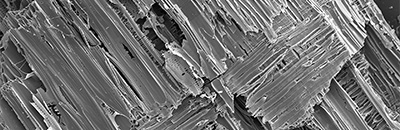
A scanning electron microscope (SEM) scans a focused electron beam over a surface to create an image. The electrons in the beam interact with the sample, producing various signals that can be used to obtain information about the surface topography and composition.
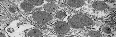
Scanning transmission electron microscopy (STEM) is an advanced imaging technique that is used to visualize the structure and composition of materials at nanometer to sub-atomic length scales. It provides data by scanning a focused electron beam across a thin sample and collecting various signals in parallel.
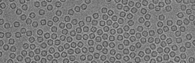
Transmission electron microscopy (TEM) is an analytical technique used to visualize the smallest structures in matter. Unlike optical microscopes, which rely on light in the visible spectrum, TEM can reveal stunning detail at the atomic scale by magnifying nanometer structures up to 50 million times.
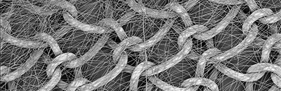
Electrospinning and electrospraying are voltage-driven fabrication processes governed by an electrohydrodynamic phenomena where fibers and particles are made from a polymer melt/solution.
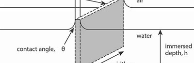
Tensiometry is the measure of surface tension, contact angles, density and other properties in order to obtain information on the interactions between gas, liquid and solid phases.
Quartz Crystal Microbalance (QCM) is an extremely sensitive mass balance that measures nanogram to microgram level changes in mass per unit area. The heart of the technology is a quartz disc. Quartz is a piezoelectric material that can be made to oscillate at a defined frequency by applying an appropriate voltage usually via metal electrodes.
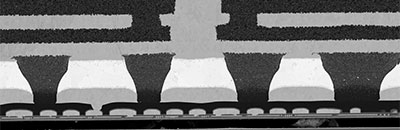
BIB milling (also known as Ion milling) is the process of removing the top amorphous layer on a material to reveal the pristine sample surface for high-resolution imaging and post-processing.
Langmuir Films are thin organic films one molecule thick and are the source of high expectations. As useful components in many practical and commercial applications such as sensors, detectors, displays and electronic circuit components. With both the possibility to synthesize custom organic molecules and sophisticated thin film deposition technology it is possible to create electrically, optically and biologically active components on a nanometer scale.