Scanning Tunneling Microscopy

The development of the family of scanning probe microscopes started with the original invention of the STM in 1981. Gerd Binnig and Heinrich Rohrer developed the first working STM while working at IBM Zurich Research Laboratories in Switzerland. This instrument would later win Binnig and Rohrer the Nobel prize in physics in 1986.

The Quantum Corral

The STM image below shows the direction of standing-wave patterns in the local density of states of the Cu(111) surface. These spatial oscillations are quantum-mechanical interference patterns caused by scattering of the two-dimensional electron gas off the Fe atoms and point defects.

Image of the Quantum Corral
Courtesy of International Business Machines Corporation. Unauthorized use not permitted
3D image of atoms taken by a Scanning Tunneling Microsope
3D rendered Scanning Tunneling Microscope image of atoms.

How an STM Works

The scanning tunneling microscope (STM) works by scanning a very sharp metal wire tip over a surface. By bringing the tip very close to the surface, and by applying an electrical voltage to the tip or sample, we can image the surface at an extremely small scale – down to resolving individual atoms.

The STM is based on several principles. One is the quantum mechanical effect of tunneling. It is this effect that allows us to “see” the surface. Another principle is the piezoelectric effect. It is this effect that allows us to precisely scan the tip with angstrom-level control. Lastly, a feedback loop is required, which monitors the tunneling current and coordinates the current and the positioning of the tip. This is shown schematically below where the tunneling is from tip to surface with the tip rastering with piezoelectric positioning, with the feedback loop maintaining a current setpoint to generate a 3D image of the electronic topography:

Schematic of Scanning tunneling microscopy
Schematic of scanning tunneling microscopy (STM).

Tunneling

Animated gif of an electon wavefunction
Schematic of electron wavefunction.

Tunneling is a quantum mechanical effect. A tunneling current occurs when electrons move through a barrier that they classically shouldn’t be able to move through. In classical terms, if you don’t have enough energy to move “over” a barrier, you won’t. However, in the quantum mechanical world, electrons have wavelike properties. These waves don’t end abruptly at a wall or barrier, but taper off quickly. If the barrier is thin enough, the probability function may extend into the next region, through the barrier! Because of the small probability of an electron being on the other side of the barrier, given enough electrons, some will indeed move through and appear on the other side. When an electron moves through the barrier in this fashion, it is called tunneling.

Quantum mechanics tells us that electrons have both wave and particle-like properties. Tunneling is an effect of the wavelike nature.

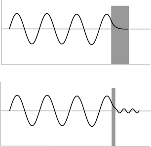
The top image shows us that when an electron (the wave) hits a barrier, the wave doesn’t abruptly end, but tapers off very quickly – exponentially. For a thick barrier, the wave doesn’t get past.

The bottom image shows the scenario if the barrier is quite thin (about a nanometer). Part of the wave does get through and therefore some electrons may appear on the other side of the barrier.

Because of the sharp decay of the probability function through the barrier, the number of electrons that will actually tunnel is very dependent upon the thickness of the barrier. The current through the barrier drops off exponentially with the barrier thickness.

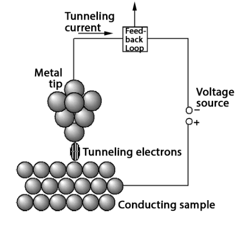
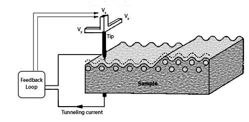
To extend this description to the STM: The starting point of the electron is either the tip or sample, depending on the setup of the instrument. The barrier is the gap (air, vacuum, liquid), and the second region is the other side, i.e. tip or sample, depending on the experimental setup. By monitoring the current through the gap, we have very good control of the tip-sample distance.

Piezoelectric Effect

The piezoelectric effect was discovered by Pierre Curie in 1880. The effect is created by squeezing the sides of certain crystals, such as quartz or barium titanate. The result is the creation of opposite charges on the sides. The effect can be reversed as well; by applying a voltage across a piezoelectric crystal, it will elongate or compress.

These materials are used to scan the tip in an scanning tunneling microscopy (STM) and most other scanning probe techniques. A typical piezoelectric material used in scanning probe microscopy is PZT (lead zirconium titanate).

Diagram of the feedback loop of a Scanning Tunneling Microscope
Feedback loop and electron tunneling for scanning tunneling microscopy (STM).

Feedback Loop

Electronics are needed to measure the current, scan the tip, and translate this information into a form that we can use for STM imaging. A feedback loop constantly monitors the tunneling current and makes adjustments to the tip to maintain a constant tunneling current. These adjustments are recorded by the computer and presented as an image in the STM software. Such a setup is called a constant current image.

In addition, for very flat surfaces, the feedback loop can be turned off and only the current is displayed. This is a constant height image.

Want to learn more? Talk to a scientist:

This site is protected by reCAPTCHA and the Google Privacy Policy and Terms of Service apply.