What is Transmission Electron Microscopy?
Transmission electron microscopy (TEM) is an analytical technique used to visualize the smallest structures in matter. Unlike optical microscopes, which rely on light in the visible spectrum, TEM can reveal stunning detail at the atomic scale by magnifying nanometer structures up to 50 million times. This is because electrons can have a significantly shorter wavelength (about 100,000 times smaller) than that of visible light when accelerated through a strong electromagnetic field, thus increasing the microscope resolution by several orders of magnitude.
TEM or STEM?
Check out this brief video to see how these two different imaging modes work to create atomic-resolution images!
To form a TEM image, a high energy electron beam is accelerated through an extremely thin “electron transparent” sample, typically thinner than 100 nm. A series of electromagnetic lenses and apertures are placed throughout the microscope’s column to focus the beam on the sample, minimize distortions, and magnify the resulting image onto a phosphor screen or a specialized camera.
A TEM comes in many different forms, but all share the same fundamental principles and components. The two major types of TEM instruments are the conventional TEM (also referred to simply as TEM) and the STEM (scanning transmission electron microscope). Other variations of TEMs include the AC-S/TEM (where AC stands for “aberration corrected”) and the E-S/TEM (where E stands for “environmental”).
Since the first demonstration of electron optics in the early 1930s, nearly a century of research and development has culminated, establishing TEM as an indispensable technique for both materials and life science applications. The most powerful modern day TEMs are equipped with modifications and additional detectors that not only push the performance and stability of the microscope but offer the added capability to collect chemical and electronic information at sub-nanometer length scales from a wide range of materials.
What is Transmission Electron Microscopy Used For?
Countless discoveries and innovations have been driven by applying TEM to the world around us. The ability to “see” atoms enable scientists to understand materials and biological systems at the most fundamental level. TEM images not only hold immense scientific value but are forms of art on their own.
TEM for Materials Science and Nanotechnology
Zooming into the atomic scale allows scientists to view the fundamental building blocks of functional materials like catalyst nanoparticles, batteries, and semiconductor devices. Focused electron beams can also be used to manipulate materials in situ, allowing “nanofabrication” and novel phenomena to be studied and discovered. The level of detail on this scale is nothing short of stunning and provides a way for understanding the connections between structure, property, and performance, allowing engineers to design nanomaterials from the bottom up.
TEM for Life Science
The world of biology is full of fascinating and dynamic yet invisible phenomena. Cryogenic TEM allows structural biologists to visualize the architecture of macromolecular assemblies like proteins, viruses, and intracellular structures at near atomic resolution. Recent technological advancements such as the use of direct electron detectors, automation, and data processing have propelled the technique into the mainstream. Using a method known as single particle analysis, scientists have been able to determine the structure of the novel coronavirus spike protein, which allows the virus to bind to host cells, allowing targeted vaccines to be developed [1].
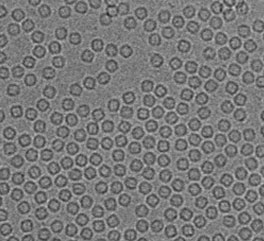

TEM micrograph of apoferritin particles and the 3D reconstruction, at a calculated resolution of 2.5 Å, generated by cryo-EM analysis using a vitrified sample prepared with the Vitrojet [9].
Components of the Transmission Electron Microscope
TEMs are composed of five key components:
- High voltage source
- Vacuum system
- Microscope column
- Detectors (e.g., imaging cameras, spectrometers)
- Control computers and software
Accelerating Voltage
Is the electric field potential applied to the electron gun to accelerate the electron beam through the microscope column and ultimately the sample. Higher accelerating voltages correspond to smaller electron wavelengths and improved resolution.
At the top of the column is the electron gun which couples to a high voltage source used to set the kinetic energy of the electron beam. Typical accelerating voltages range from 80 kV up to 300 kV. The microscope column consists of a series of electromagnetic lenses and apertures to focus the electron beam onto the sample and magnify the TEM image onto the viewing screen (or detectors). A vacuum system is used to maintain the required vacuum levels throughout the column. Due to the complexity of the instrumentation, most of the components are automatically computer controlled with only a few key parameters controlled by the microscopist. The main user-controlled settings include the sample stage position, magnification, objective lens current, beam current (spot size), and the choice of which apertures and detectors to use when acquiring data.
Modern TEMs are equipped with electronic detectors (such as charge coupled device, or CCD, detectors), in addition to a retractable fluorescent viewing screen, to capture TEM images in a digital format. Most TEMs will also include an X-ray detector that can be inserted between the objective lens pole-pieces (near the sample) to analyze composition. Optional electron energy-loss spectrometers located at the end of column are used for electron energy-loss spectroscopy (EELS).
Vacuum system
To eliminate electron beam interactions with anything but the specimen, a high vacuum system is connected to the column [2]. Typical TEMs will employ three types of vacuum pumps:
- Roughing pumps pump down from atmospheric pressure down to a “low” vacuum level (around 0.01 mbar). These pumps are very loud because they are mechanically pumping relatively large volumes of air. The roughing pump is often used multiple times during a session to pump out the specimen load lock chamber before it enters the ultra-high vacuum environment of the column. Roughing pumps are also used to “back” certain high vacuum pumps, providing an additional layer of pumping.
- One or more types of high vacuum pumps that require “backing” by a rough pump to reach ultra-high vacuum levels (i.e., 10-5 to 10-10 mbar). Examples include turbo pumps or diffusion pumps. These pumps are used for pumping down the column. Once the column reaches the required vacuum level, the backing or roughing pump is usually turned off to reduce mechanical vibrations and will automatically trigger every few hours for a short period of time to pump out accumulated gas.
- One or more high vacuum pumps that do not require backing – such as an ion pump. The ion pump is used for maintaining ultra-high vacuum in the gun chamber. A differential pumping aperture is used to separate the gun chamber, pumped by the ion pump, from the rest of the column in order to protect the electron gun from degrading.
Some TEMs will have additional types of pumps known as “getters” or “traps” for high and low vacuum ranges, respectively. These allow certain gas species to adsorb on a chemically reactive surface. Cryogenic pumps such as “cold fingers” are often positioned within the objective lens pole piece (i.e., within the sample vicinity) to freeze stray gas molecules to its surface. A small liquid nitrogen dewar outside the microscope column is filled at the beginning of a session (and sometimes refilled during sessions) to maintain performance.
Pressure and Vacuum
The TEM needs to be kept permanently under vacuum unless it is being serviced or repaired. Samples are inserted and removed via an airlock system that takes the pressure from atmosphere (~ 105 Pa) down to ~10-5 Pa in a matter of minutes – truly extraordinary!
Electron Gun
One of the most important parts of the TEM is the electron source, often called the electron “gun”. The electron source needs to meet certain requirements to produce high resolution images. There are two main types of electron guns for TEM: thermionic and field emission. The characteristics of the emitter will determine the resolution limit of the microscope, which depend upon the brightness (i.e., current density per unit solid angle of the source), spatial coherence, and temporal coherence.
Coherent or Incoherent?
The wave nature of electrons means that individual electrons emitted from the gun can be coherent or incoherent. The ideal case is a perfectly coherent beam composed of electrons that are all “in-step” with one another. Deviations from this ideal state can be described in terms of spatial and temporal coherence, which will ultimately determine the resolution limit [3].
Temporal coherence length: λc = v h/ΔE
ν = electron velocity, h = Plack’s constant, ΔE = energy spread of the beam
Spatial coherence length: dc = λ/2α
λ= electron wavelength (i.e., accelerating voltage), α = angle subtended by the source at the specimen (can be modified by a condenser aperture)
Compared to tungsten, ceramic crystals can emit electrons at a lower temperature which leads to a brighter beam (i.e., higher current density) with less energy spread (i.e., better temporal coherence). These are more expensive than tungsten and require higher vacuum levels but support longer lifetimes and better spatial resolution.
Field emission guns (FEGs) rely on a different yet simpler mechanism to emit electrons, namely tunneling. An electrical field is applied via the first anode (Anode 1) to an extremely sharp and pointed tip made of tungsten to induce tunneling. The second anode (Anode 2) accelerates the electrons to the specified accelerating voltage. No Wehnelt cylinder is needed as the two anodes act together to focus the beam. The result is a significantly brighter and coherent beam than any thermionic emitter, making them ideal for high resolution S/TEM applications.
The two types of FEG sources are cold FEGs and Schottky FEGs. A cold FEG relies purely on tunneling to generate electrons whereas the Schottky type is assisted by thermionic emission. This is achieved by coating the tungsten tip with a thin layer of zirconium oxide (ZrO) which lowers the work function thus promoting thermal emission of electrons.

Comparison of Electron Gun Characteristics [3]
| Crossover size (nm) | Brightness (A/m2sr) | Energy spread at 100 kv (eV) | Emission current stability (%/h) | Lifetime (hr) | |
| TUNGSTEN (Thermionic) | >105 | 1010 | 3 | <1 | 100 |
| LAB6 | 104 | 5 x 10¹¹ | 1.5 | <1 | 1000 |
| SCHOTTKY FEG | 15 | 5 x 10¹² | 0.7 | <1 | >5000 |
| COLD FEG | 3 | 1013 | 0.3 | 5 | >5000 |
Illumination system
The illumination system takes the beam from the electron gun and guides it to the sample, either in the form of a broad “parallel” beam for TEM or a small, focused probe for STEM. To do this, a combination of two condenser lenses and at least one aperture at the exit plane of the second condenser lens (in combination with tilt and deflection coils) are needed.
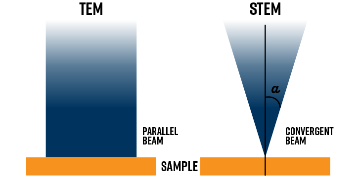
In TEM mode, the condenser lenses are adjusted to form a broad beam at the sample that is several micrometers in diameter [3]. The upper pole piece of the objective lens can act as a third condenser lens to create an even more parallel beam. This is ideal for generating sharp diffraction patterns and stronger image contrast.
For STEM mode, the opposite is needed. Instead, the illumination system acts to form a convergent beam (probe) at the specimen entrance surface. Images are formed by scanning the focused probe across the field of view. The condenser aperture is inserted to define the probe’s convergence angle, α.
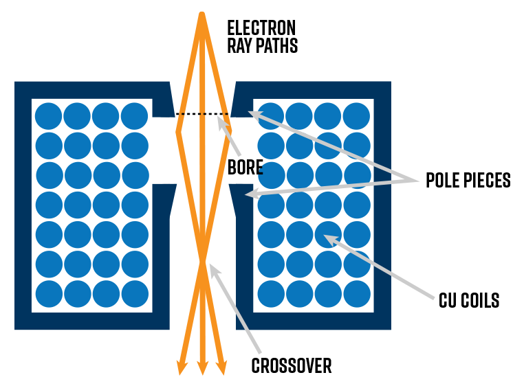
Electromagnetic lenses
Electromagnetic lenses are composed of two major components: the copper wire coils and the pole piece(s). Current passing through the coils creates a magnetic field within the column. The magnetic field is asymmetric: weakest in the center and strongest toward the edges, which acts to focus off-axis electrons and form the beam cross-over.
Objective Lens
The most important lens in the TEM is the objective lens. It forms the images and diffraction patterns (DPs) that are magnified onto the viewing screen or camera.
By analogy to light optics, an image is characterized by a one-to-one correspondence between points in the image and points in the object. In the case of TEM images, the object is the transmitted electrons just at the exit surface of the specimen. The objective lens disperses the electrons emerging from the exit-side of the specimen in the back focal plane (BFP), where the diffraction pattern is found, and recombines them in the image plane. To generate the high-resolution images of atomic columns, the focal length of the objective lens must be minimized to maximize magnification. Thus, the object distance, or distance between the specimen and the objective lens must be very small.
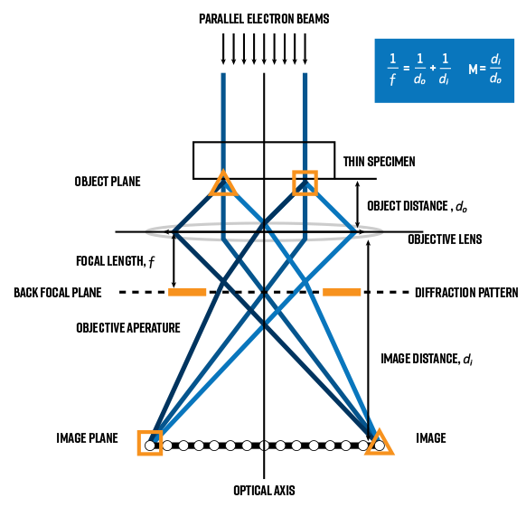
Due to these specific requirements, the construction of the objective lens is more complex than the other lenses in the column. So called “split” constructions allow separate sets of coils to independently control the field strength in the upper and lower pole-pieces. Not only does this geometry provide space for insertion of the sample close to the objective lens within the pole-piece gap, thus minimizing the object distance, but it also accommodates the insertion of X-ray spectrometers along with a variety of sample holders (e.g., double-tilt, in-situ, cooling, etc).
Split designs are also advantageous for switching between TEM and STEM modes. The upper pole piece current can be independently adjusted to form the convergent probe in STEM mode. In TEM mode, the lower objective lens pole piece is responsible for image formation (while the upper pole piece aids in parallel beam formation).
It’s important to note that the objective lens should operate at a constant current that minimizes lens aberrations. As a result, focus is achieved by adjusting the “Z-height” of the specimen via the goniometer. A term known as the eucentric plane is used to define the standard object plane for the objective lens. When the specimen height is in the eucentric plane, the image will be in focus and the objective lens will have a standard reference value.
Objective Lens aberrations and practical resolution
In TEM mode, the actual resolution is determined by the objective lens’ ability to form an image of the object. In STEM mode, resolution is governed by how small and bright the convergent probe is. In either case, lens aberrations (i.e., imperfections) limit the resolution.
Intermediate and projector lenses
The intermediate and projector lenses magnify the image or diffraction pattern onto the viewing screen. Multiple intermediate lenses are used to adjust the degree of magnification of the image or DP produced by the objective lens. The projector lens is the final lens in the column that projects the image/DP onto the viewing screen or camera.
Electron-Sample Interactions
In order to identify the right imaging approach or correctly interpret image contrast or spectral characteristics, it’s important to understand all of the relevant signals originating in the TEM. All the signals generated in the TEM either originate from elastic scattering or inelastic scattering.
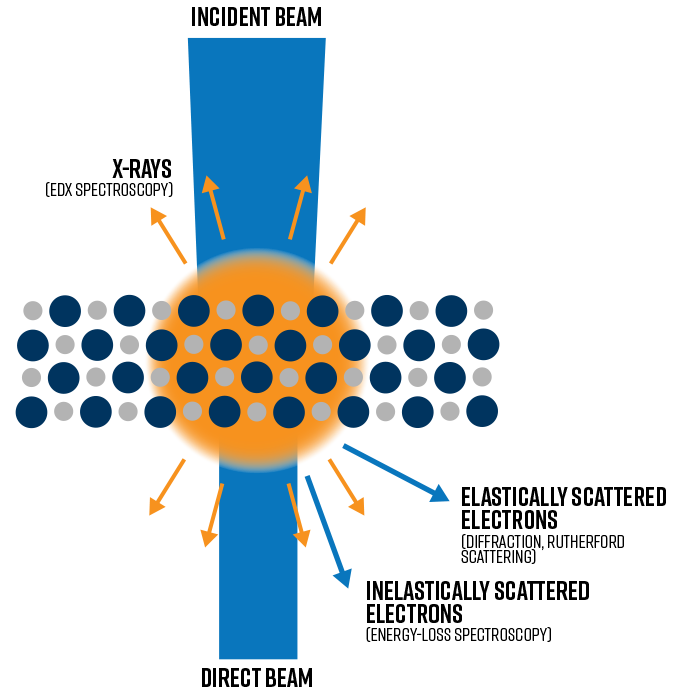
Elastic scattering
Elastic scattering events involve no energy transfer to the incident electrons. Two types of interactions with isolated atoms result in elastic scattering:
- Interaction with the electron cloud results in low angle scattering.
- Coulombic attraction to the positively charged nucleus results in high angle (Rutherford) scattering.
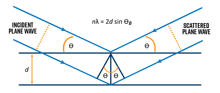
In real TEM samples which are often crystalline materials, atoms are arranged in a repeatable 3D arrangement (lattice structure). When the electron beam enters the crystal, elastic scattering will occur at characteristic angles corresponding to the unique lattice spacings (also called d spacings) in that material.
These characteristic scattering angles are also referred to as Bragg angles. As a result, the diffraction pattern captures an imprint of the Bragg angles and conveys information about the crystalline structure of the material such as symmetry, lattice spacings, strain, and defects. For polycrystalline or amorphous materials, the diffraction pattern becomes a series of diffuse rings wherein the ring radii correspond to the lattice spacings, and the magnitude of diffuseness increases with decreasing average crystallite size.
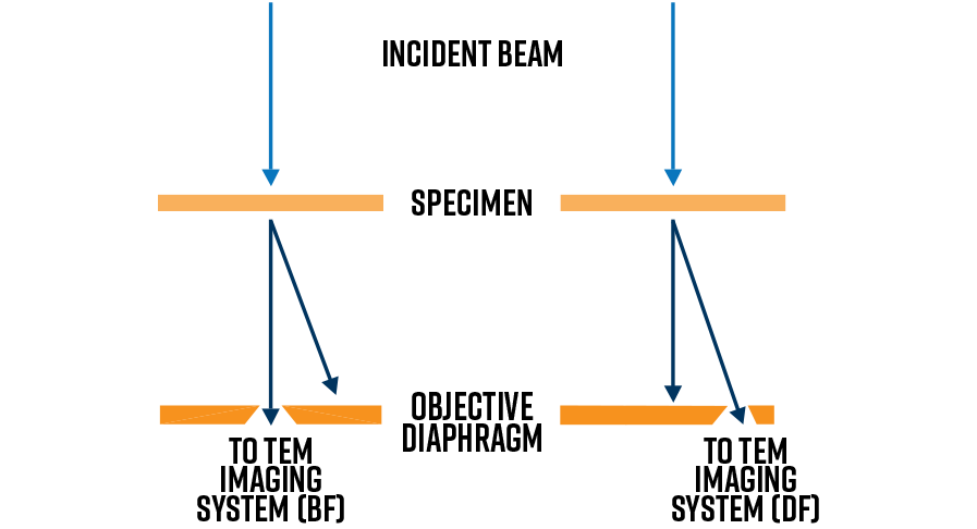
Amplitude contrast TEM images
The amplitude of the transmitted electron (waves) can be altered by two mechanisms:
- Mass-thickness variations in the sample across the field of view.
- Inhomogeneities in the diffracting (Bragg) conditions across the field of view.
Variations in the sample’s mass or thickness (or both) will alter the amplitude of electrons transmitting the sample through Rutherford (thermal diffuse) scattering. This type of scattering occurs at high angles. Therefore, by placing the objective aperture around the direct beam (optic axis), these high-angle-scattered electrons are excluded from the image plane and hence a bright field (BF) image is formed. The BF image demonstrates mass-thickness contrast and hence is dark is areas of higher mass-thickness.
Diffraction contrast images are generated by excluding all electrons except those scattered to a particular Bragg angle. The objective aperture is placed about a selected Bragg beam (lattice spacing) which results in a dark field (DF) image. Amplitude contrast occurs when the diffracting conditions for a particular Bragg angle changes across the field of view. Therefore, slight changes in the crystalline orientation (i.e., Bragg condition) can be deduced by DF contrast. In practice, the best way to get a DF image is by tilting the specimen to a so called “two-beam” condition wherein the direct beam and only one Bragg beam is strongly excited.
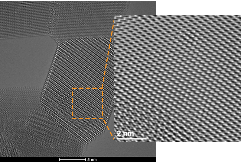
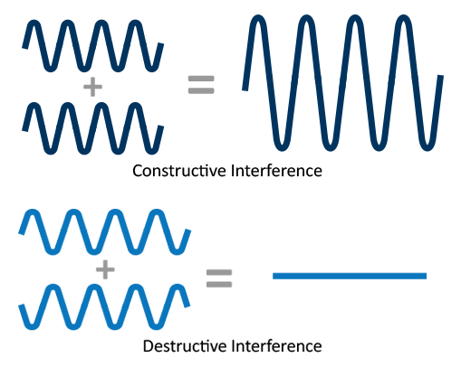
Phase Contrast TEM Images
Phase contrast occurs when multiple beams, such as the direct and Bragg beams, constructively and destructively interfere because of relative phase shifts. This phenomenon gives rise to lattice fringes observed in HR-TEM images, Fresnel fringes about the specimen edges, or Moiré patterns. Phase contrast images give rise to the highest spatial resolution because multiple beams, and those scattered to higher angles (smaller d-spacings) are included.
Interpreting phase contrast images
While phase contrast images one way to acquire atomically resolved TEM images, they can be especially difficult to interpret without an extremely thin sample. This is because phase contrast is sensitive to changes in sample thickness, sample tilt, focus, and lens aberrations. If the sample is very thin and the electron-optical parameters are well known, then image simulation can be used for structural interpretation.
Selected Area Diffraction
Another useful mode in the TEM is to use the selected area aperture to generate a selected area diffraction (SAD) pattern. This is the most useful way to collect a high-quality diffraction pattern because the sample may be buckled across the entire field of view, causing distortions in the DP. Since the SAD aperture is located in the image plane of the objective lens, inserting a SAD aperture allows microscopists to only include electrons from a local area defined by the SAD bore diameter.
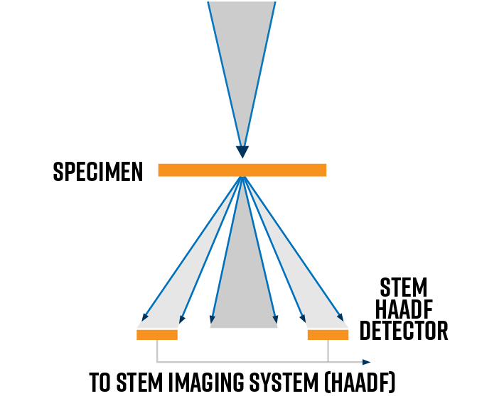
High-Angle Annular Dark Field (HAADF) STEM Images
In STEM mode, atomically resolved mass-thickness contrast images can be generated by using a high-angle annular dark field (HAADF) detector. This detector collects the Rutherford scattered electrons ejected to high scattering angles. As the convergent probe scans the field of view, the HAADF detector collects the signal intensity at each point and effectively maps the atomic column positions.
Inelastic scattering
Unlike elastic scattering, inelastic scattering is characterized by a measurable loss of energy to the incident electrons – on the order meV (1000 meV = 1 eV) up to several hundred eV, which represent a small fraction of the incident beam energy.
There are many types of signals in TEM that arise from inelastic scattering. Pairing this data along with high resolution images provides powerful, correlative data that only a S/TEM can deliver. This “holistic” approach to materials characterization that the modern-day S/TEM provides (namely the ability to perform analytical nano-analysis of composition, chemistry, and bonding) is what makes the technique so useful for nanotechnology and materials science applications.
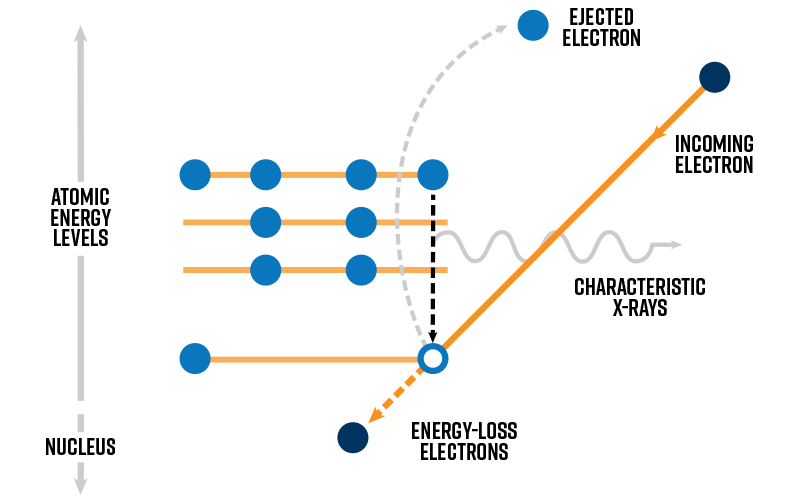
Inelastic scatter generates energy-loss electrons, X-ray emission, secondary electron emission, and sometimes visible light emission (i.e., cathodoluminescence or CL). The two most popular inelastic signals analyzed in the TEM are energy-loss electrons measured via electron energy-loss spectroscopy (EELS), and characteristic X-rays detected with energy-dispersive X-ray spectroscopy (i.e., EDS or EDX spectroscopy).
X-ray Spectroscopy
X-ray spectroscopy is one of the most popular chemical analyses that can be performed in the TEM or STEM. An EDX spectra provides a snapshot of the elements present in the sample. There are two types of X-rays produced via inelastic scattering:
- Characteristic X-rays: used for compositional analysis in nano-sized regions like defects, surfaces, precipitates, and interfaces.
- Bremsstrahlung X-rays: translates from German to “braking radiation” is a type of continuum X-ray emission involving inelastic interaction with atomic nuclei. It is commonly used in biological applications.
Characteristic X-rays are produced when an incident electron penetrates to the inner-shell electrons. If enough energy is transferred from the incident electron to the inner-shell electron, then the atom in the sample will become ionized. This excited state involves a “hole” being left behind in the inner shell. For the atom to relax back to the ground state, it must fill the hole with an outer-shell electron by emitting an X-ray with the same energy as the energy difference between the inner and outer shells. Because each element has unique energy levels within each electron shell, characteristic X-rays are representative of the sample composition.
Bremsstrahlung X-rays occur when fast electrons penetrate through all electron shells and interact inelastically with the charge field of the nucleus. Unlike characteristic X-rays, energy-loss resulting from this interaction can be any energy below the upper-bound kinetic energy of the incident beam. Characteristic X-rays are superimposed on this continuum signal in the EDX spectra. For biologists, the Bremsstrahlung intensity can be useful for understanding the average atomic number of the specimen. For materials science applications, the Bremsstrahlung is typically regarded as a background signal that obscures the characteristic X-rays.
The emission of characteristic X-rays from the thin specimen is isotropic. On the other hand, Bremsstrahlung emission is anisotropic in the forward direction (i.e., concentrated at the exit-surface side of the specimen). This fact can be leveraged to enhance the signal strength for elemental analysis. The EDX detector is inserted in between the pole-piece gap (above the sample) and tilting of the sample toward the EDX detector further helps to improve signal-to-noise.
Electron energy-loss spectroscopy
EELS measures the energy distribution of all electrons that have interacted inelastically within the sample [4]. Unlike X-ray spectroscopy, which detects de-excitation events, the EEL spectrum represents excitations or ionization within the specimen and therefore can probe a wider variety of phenomena than EDX spectroscopy. These include core-shell transitions, plasmon resonance, valence-to-conduction band transitions in semiconductors, and even vibrational modes (phonons).
Lens Aberrations
The diffraction limited resolution of the TEM is far better than the practical resolution for a variety of reasons. These can include mechanical vibrations in the microscope room, acoustic interferences, unstable high voltage sources, and thick samples – all of which serve to degrade the practical resolution. Once these roadblocks are overcome (a relatively easy process at an advanced TEM facility), the reality of objective lens aberrations will ultimately limit microscope resolution. The two main types of objective lens aberrations that limit microscope resolution are known as spherical and chromatic aberrations.
Spherical aberration
Spherical aberration, commonly referred to as “Cs” for the spherical aberration coefficient, is present in all round electromagnetic lenses (the objective lens is considered a “round” lens). It impacts off-axis electron rays by focusing these rays more strongly the further off-axis they are scattered by the specimen. As a result, points originating in the object appear as a finite disk (i.e., distorted or blurred out) in the TEM image. With this in mind, optimum resolution can be achieved by adjusting the objective lens current to a slightly “defocused” condition, meaning that the intermediate lens’ object is not on the image plane but rather slightly “above” this plane. This condition is referred to as Scherzer defocus [5].
Chromatic aberration
Chromatic aberration (Cc) has to do with the energy (wavelength, i.e., color – as an analogy to visible light) of the electrons, which are not really monochromatic as the accelerating voltage implies. Depending on the type of electron gun, the energy spread of the beam will vary from about 0.3 eV (cold FEG) to about 1 eV (LaB6 thermionic) [3]. In conventional S/TEMs, chromatic aberration does not limit spatial resolution because the relative energy spread is such a small fraction of the accelerating voltage. However, in S/TEMs that are equipped with Cs correctors, the next thing that limits practical resolution are the chromatic aberrations.
Another way in which chromatic aberration can arise is due to inelastic scattering within thick specimens. This generates energy-loss electrons and further increases the energy spread of the beam that exits the sample. The effect worsens with specimen thickness, which is another reason why extremely thin samples (<100 nm) are preferred for high resolution imaging and nano-analysis.
There are two ways to minimize chromatic aberration. The first and most direct approach is limiting the specimen thickness. Another way to minimize chromatic aberration are through beam monochromators, which can reduce the energy spread to a few meV, which is about a factor of 100 times better than a cold FEG gun’s energy spread. The use of monochromators in STEM-EELS has enabled microscopists to detect phonons, or vibrational modes, within crystals and other materials with nanometer spatial resolution [7].
Strengths and Limitations of Transmission Electron Microscopes
While TEM is a highly versatile technique with a wide variety of applications, it is important to note the limitations of TEM in addition to noting its many strengths. By understanding the potential disadvantages of TEM and STEM, microscopists can not only better understand the complex data generated by these instruments but also develop new approaches that address certain limitations, thereby expanding the utility of the technique.
Advantages
- Offers the highest and most powerful magnification of any microscopy technique.
- Versatile imaging modes: dark/bright field and phase contrast (TEM); high-angle annular dark field (STEM).
- Provides the ability to collect electron diffraction patterns (crystallographic information) from nanometer-sized regions by using selected-area diffraction (SAD).
- Enables nano-analysis: the ability to collect local information about composition and bonding which can be correlated to high resolution images.
Disadvantages
- Limited sampling: a typical field of view for a HR-TEM image is no more than 100 nm2.
- Complex image interpretation: all TEM images (and diffraction patterns) are 2D projections of 3D structures.
- Possibility of electron beam damage, especially for light elements, biological samples, and soft materials. In many cases, this makes it challenging to collect meaningful data before the sample is amorphized.
- Specialized techniques that utilize advanced equipment like cryo-TEM, low dose TEM, low-kV TEM can be leveraged to analyze beam sensitive materials.
- Vacuum environment required – limiting the ability to observe functional materials under realistic “working” conditions.
- E-TEMs and in situ TEM holders can be used to probe materials under stimuli (heat, gas, liquid, electrical bias).
- Difficult sample preparation to create extremely thin specimens; thin samples often result in imaging artifacts.
References
[1] D. Wrapp, N. Wang, K. S. Corbett, J. A. Goldsmith, C.-L. Hsieh, O. Abiona, B. S. Graham and J. S. Mclellan, “Cryo-EM structure of the 2019-nCoV spike in the prefusion conformation,” Science, vol. 367, no. 6483, pp. 1260-1263, 2020.
[2] J. Rodenburg, “The Vacuum System,” [Online]. Available: http://www.rodenburg.org/guide/t1400.html. [Accessed August 2022].
[3] D. B. Williams and C. B. Carter, Transmission Electron Microscopy, Springer, 2009.
[4] R. Egerton, Electron Energy Loss Spectroscopy in the Electron Microscope, New York: Springer, 1996.
[5] O. Scherzer, “Theoretical Resolution Limit of the Electron Microscope,” Journal of Applied Physics, vol. 20, no. 20, 1949.
[6] C. Jia, L. Houben, A. Thust and J. Barthel, “On the benefit of the negative-spherical-aberration imaging technique for quantitative HRTEM,” Ultramicroscopy, vol. 110, no. 5, pp. 500-505, 2010.
[7] O. Krivanek, T. Lovejoy, .. Dellby, T. Aoki, R. Carpenter, P. Rez, E. Soignard, J. Zhu, P. Batson, M. Lagos, R. Egerton and P. Crozier, “Vibrational Spectroscopy in the Electron Microscope,” Nature, vol. 514, pp. 209-214, 2014.
[8] L. Ruiz-Perez, G. Marchello, C. D. Pace, S. Acosta-Gutierrez, G. Ing, N. Wilkinson, F. Gervasio, G. Battaglia, F. Werner and S. Pilotto, “Imaging protein conformational space in liquid water,” BioRxiv, 2021.
[9] R. B. G. Ravelli, F. J. T. Nijpels, R. J. M. Henderikx, G. Weissenberger, S. Thewessem, A. Gijsbers, B. W. A. M. M. Beulen, C. López-Iglesias and P. J. Peters, “Cryo-EM structures from sub-nl volumes using pin-printing and jet vitrification,” Nature Communications, vol. 11, no. 2563, pp. 1-9, 2020.