Solutions for Semiconductor Research & Development
1. Microanalysis of IC Packaging
2. Automated Particle Analysis
3. Artifact-free Cross Sectioning
4. Interfacial Interactions
5. Chemical Mechanical Planarization
Heterogeneous integration is becoming increasingly important for achieving system-level scaling and overall semiconductor device miniaturization. Developing the next generation of advanced packaging, as well as overcoming the many challenges in this space, will require novel materials and manufacturing processes. From pathfinding to quality control and failure analysis, streamlined workflows enabled by automated solutions can help engineers accelerate the pace of innovation.
Nanoscience Instruments provides a variety of advanced yet approachable solutions for analyzing next-generation semiconductor packaging materials and devices:
Microanalysis of IC Packaging with Scanning Electron Microscopy
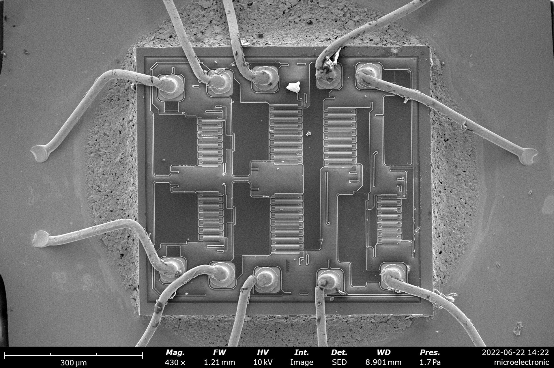
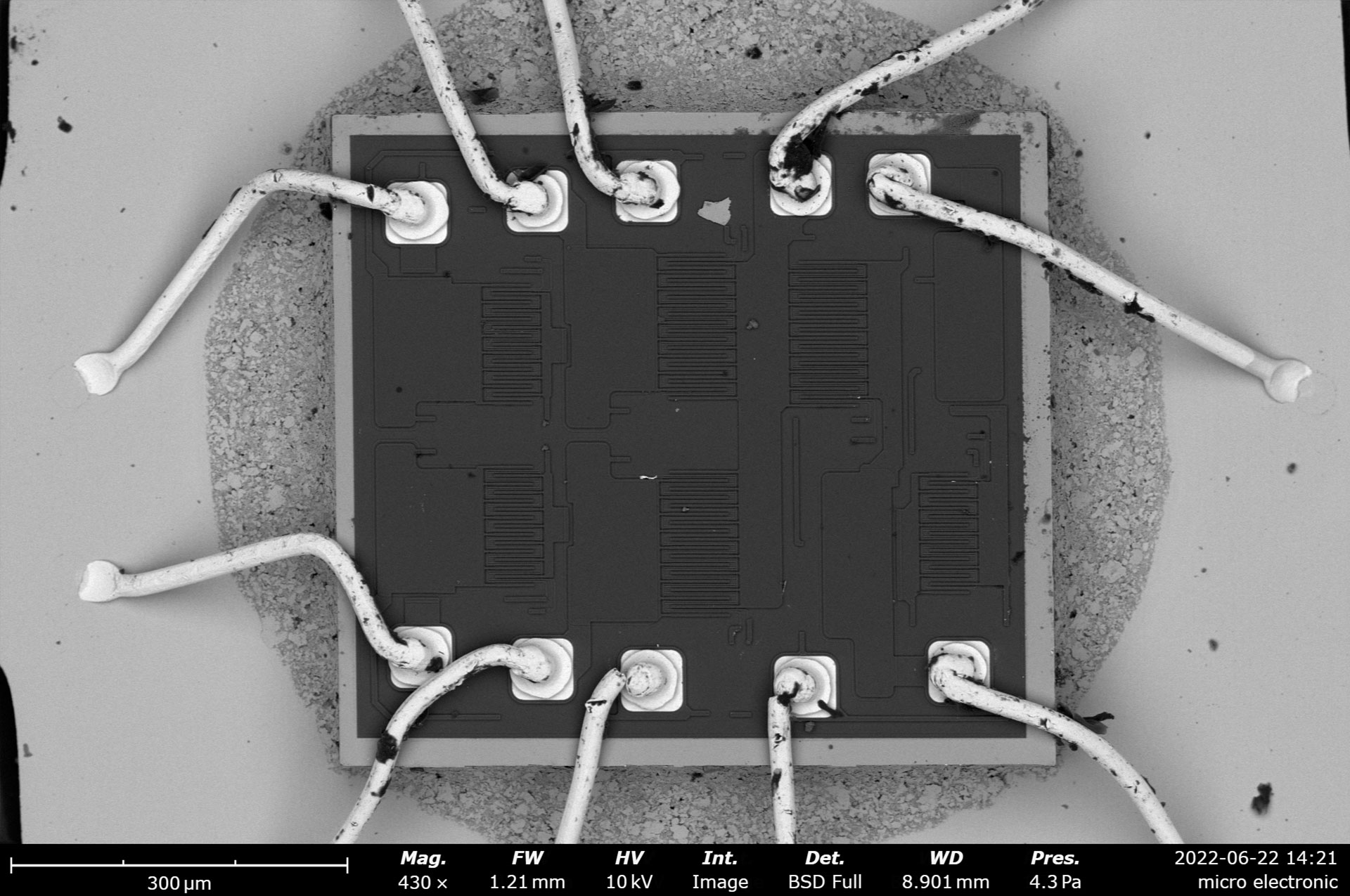
Scanning electron microscopy (SEM) is an indispensable tool in the development and failure analysis of semiconductor device packaging. Versatile imaging modes enabled by multiple detectors allow surfaces and interfaces to be visualized on micrometer and nanometer length scales with enhanced depth of focus and exceptional clarity. The wealth of data provided by SEM can be used to identify failure mechanisms such as cracks, delamination, voids, and other features that are often imperceptible through other techniques.
SEM images of a wire-bond package acquired on a Phenom ProX Desktop SEM using the SED (left), BSD (middle), and EDS (right) detectors.
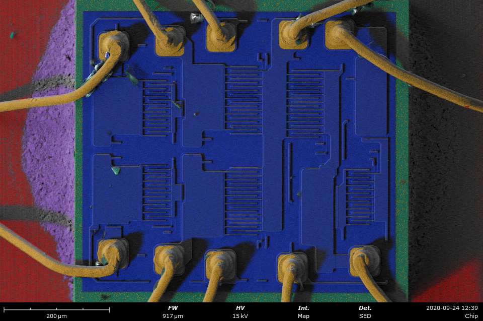
Rapid Elemental Mapping
When combined with SEM imaging, energy dispersive X-ray spectroscopy (EDS) supercharges failure analysis capabilities. EDS analyzes the X-rays emitted from the sample as the electron beam scans the sample, allowing a high-resolution map of surface elemental composition to be visualized.
The one-click elemental analysis software available on all Phenom’s paired with the high-brightness electron source and solid-state detector allows for efficient and accurate EDS acquisition, mapping, and semi-quantitative analysis.
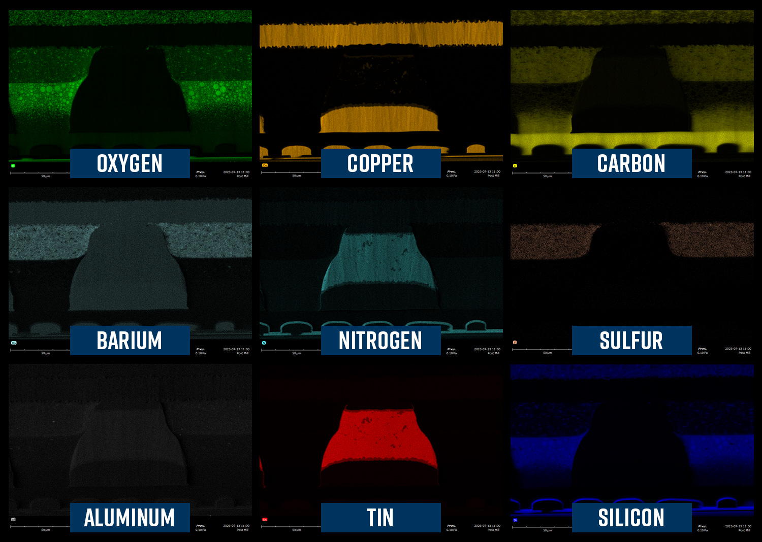
Elemental Abundance Map
This elemental map shows the distribution of several elements within a cross section of an IC package substrate. EDS mapping allows for the quick identification of elemental distributions and potential contamination.
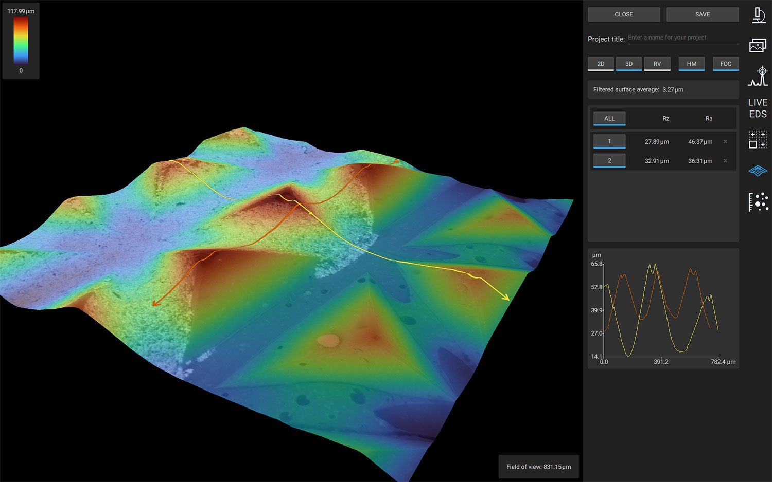
3D Surface Topographic Mapping
3D surface topography mapping involves the creation of a detailed, three-dimensional representation of a surface, allowing for unambiguous identification of peaks and valleys present on chips, substrates, or other critical packaging components. This precise microscale feature identification enables engineers to assess the quality and roughness of materials with more confidence and monitor inconsistencies in manufacturing processes.
All Phenom Desktop SEMs come standard with a 3D Roughness Reconstruction application. Made possible by the segmented backscattered electron detector (BSD), semi-quantitative 3D images and sub-micron roughness measurements can be generated from BSD images. Heat map color scales are used to represent different relative Z-heights and users can generate line scans and standard roughness metrics at the click of a button.
The Phenom 3D Roughness Reconstruction (3DRR) software can help in the interpretation of surface topography and is crucial in assessing and controlling surface quality in a variety of materials.
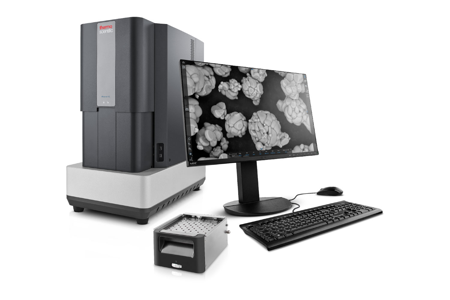
The Phenom Desktop SEM is the most intuitive and efficient SEM ever built. Its small form factor requires minimal space, allowing the placement of the Phenom at the site of need – whether it be in a laboratory or on the manufacturing floor. After loading the sample, images are a few clicks and seconds away.
Images are < 60 seconds away from loading the sample
Bright, long-lifetime CeB6 or FEG electron sources
Low cost of ownership and infrequent source changes
Opportunity for automation with predefined and customizable workflows
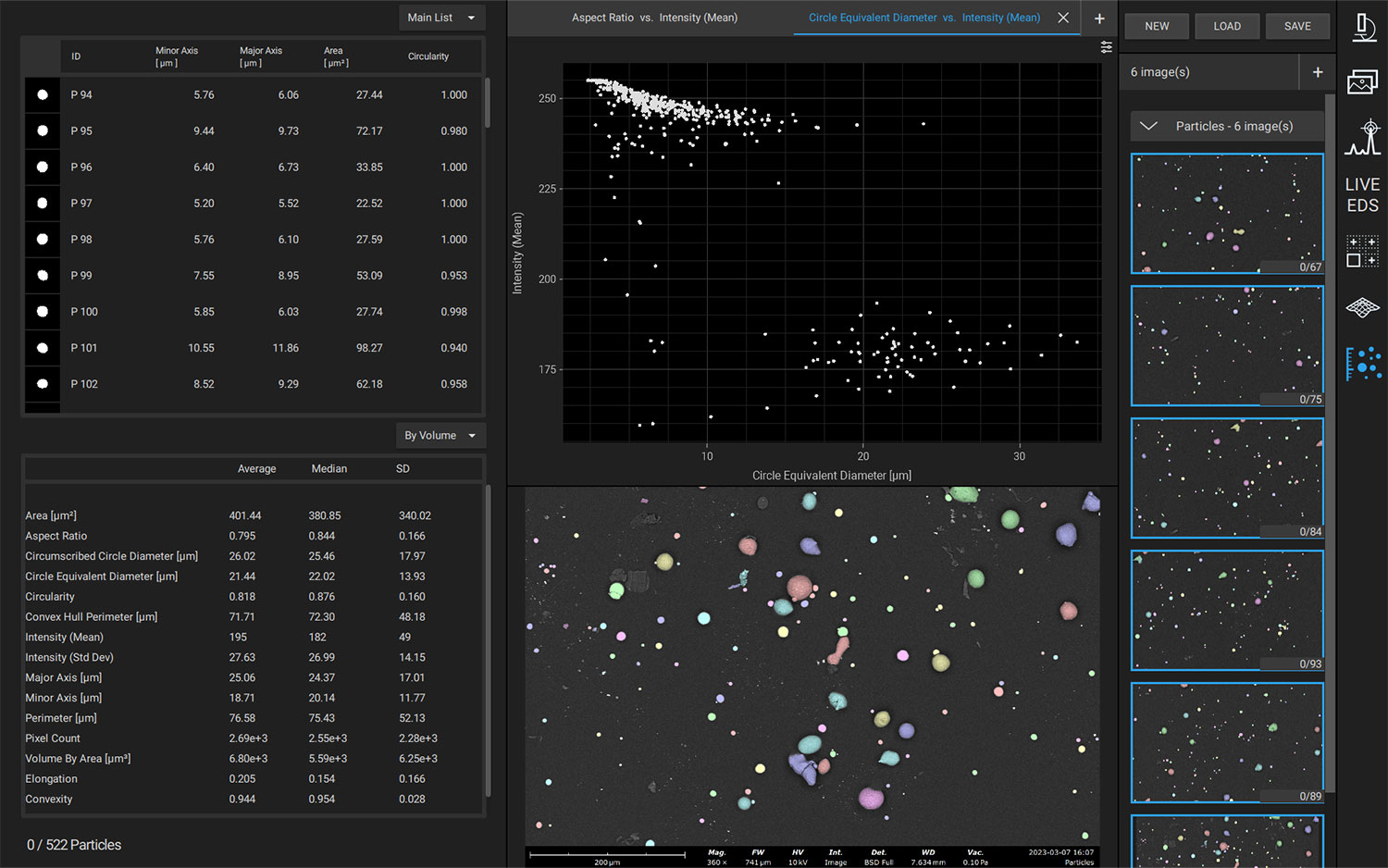
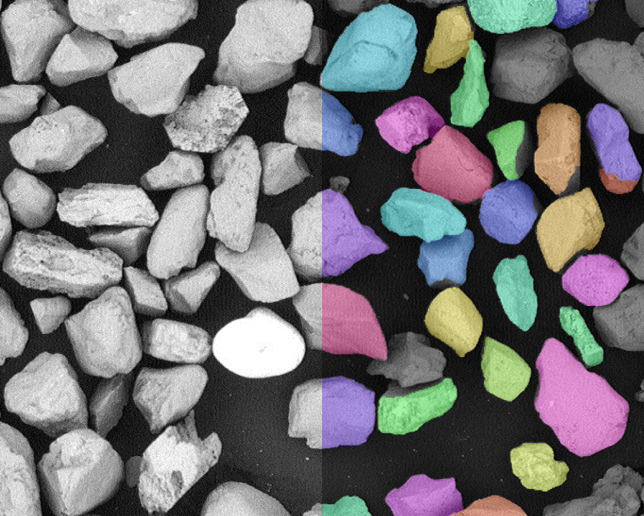
With the constant push for smaller and more powerful semiconductor devices, the detection and analysis of contaminants, defects, and foreign particles in microelectronics is crucial. SEM-based automated particle analysis streamlines this process, offering rapid, high-throughput characterization of particle sizes, composition, and morphology. This technology not only aids in identifying potential sources of defects and failures in semiconductor devices but also helps manufacturers maintain stringent quality control standards in cleanroom environments. By pinpointing and addressing particle-related issues early in the production process, SEM-based automated particle analysis contributes to higher yields, improved device reliability, and ultimately, the delivery of high-performance, fault-free semiconductor products to the market.
a
Phenom ParticleMetric image analysis software detects and analyzes up to 1000 particles per minute.
ParticleX software equips the Phenom Desktop SEM to run 24/7 and perform comprehensive particle analysis. Obtain accurate data on the size, shape, and elemental composition of thousands of particles at the push of a button, allowing you to gain rich insights on cleanroom cleanliness and narrow-down potential sources of contamination.
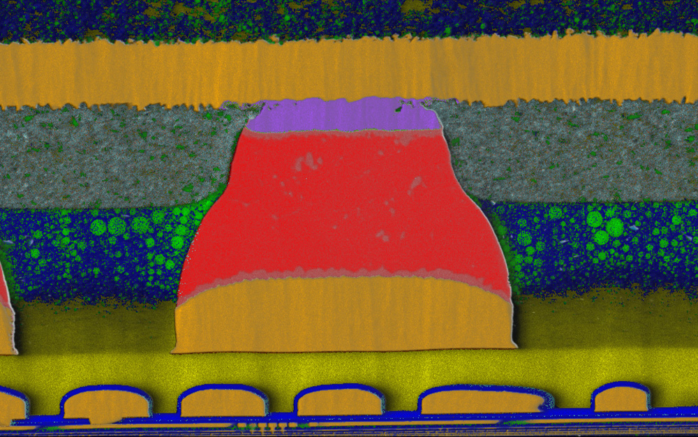
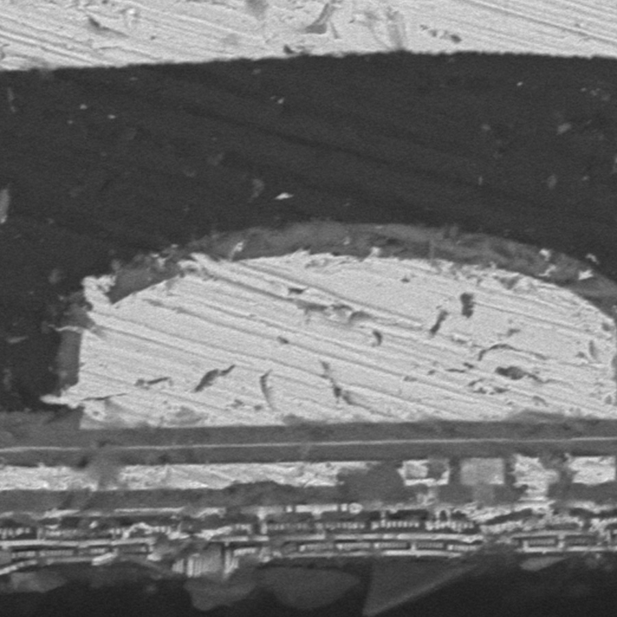
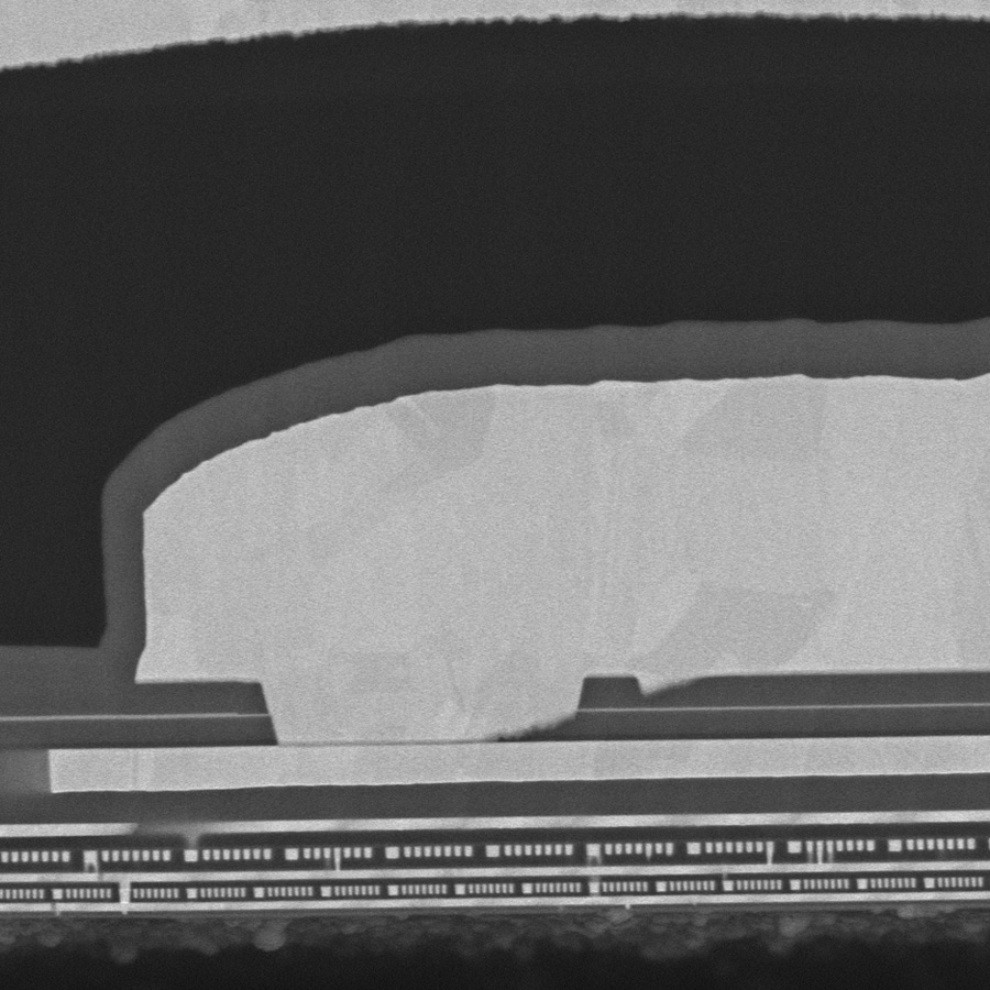
Cross sectioning is a commonly utilized sample preparation technique in semiconductor device failure analysis because it can reveal internal structures at suspected electrical failure locations. Broad beam ion milling ensures the highest quality of SEM data by revealing an artifact-free surface by gently, yet rapidly, milling away material. By offering a non-destructive means of accessing the device’s internal features, broad beam ion milling facilitates in-depth investigations, helping engineers pinpoint and address the issues responsible for the semiconductor’s failure.
A microelectronic package substrate after mechanical cross-sectioning (left) and ion milling with the SEMPrep-2 (right). Ion milling provides a smooth surface finish without damaging any of the delicate structures, allowing individual grains within the metallization layers to be detected.
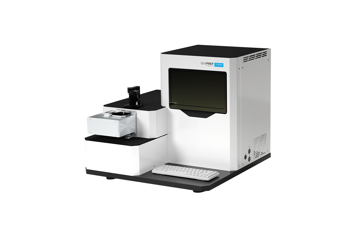
The SEMPrep SMART Ion Mill provides the greatest level of control and versatility that is crucial for all types of failure analysis and process development applications. With the fastest milling rate, dual cooling options, automated operation, and a variety of sample holders, obtaining exceptional SEM data from any microelectronic structure can be approached with confidence and efficiency.
Characterization of solid-liquid interfacial interactions
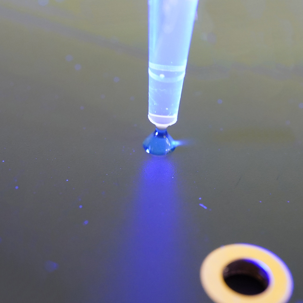
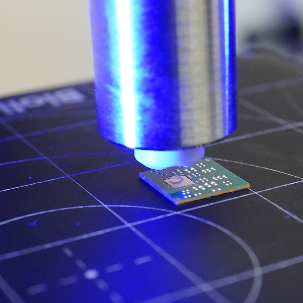
Accurate characterization of liquid-solid interactions is paramount for semiconductor packaging R&D as it underpins the successful advancement of next-generation packaging solutions, like 2.5D and 3D IC packaging. Understanding the surface energy and wettability of materials used in semiconductor packaging is crucial for selecting appropriate surface treatments, fluxes, adhesives, underfills, and encapsulants that will ensure optimal electrical conductivity, thermal dissipation, and package reliability. Precise characterization of surface and interfacial properties aids in tailoring material interactions, ensuring proper wetting and adhesion, and minimizing defects, such as voids or delamination.
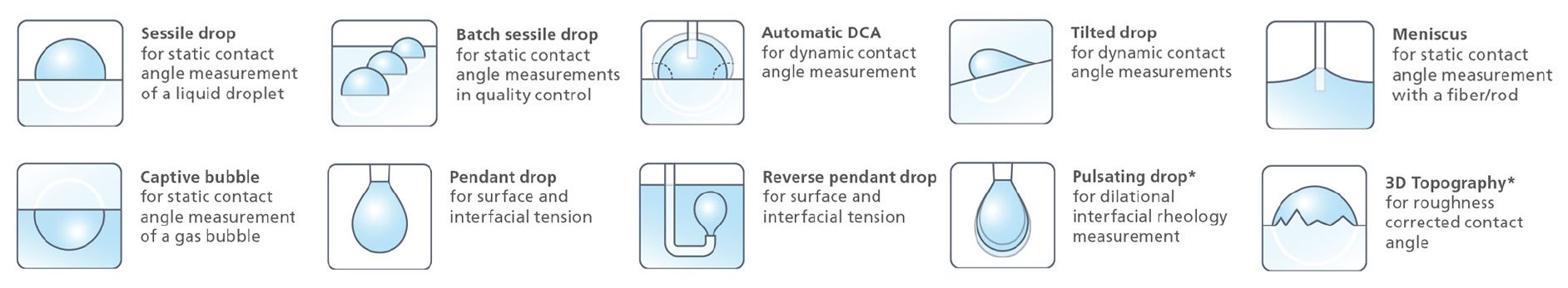
Dispense liquids on a substrate and obtain a complete range of automated measurements including contact angle, surface free energy, wettability, and many more. Heated chambers are available for conducting measurements at elevated temperatures. The Theta Wafer stage is also available for measurements on standard wafers up to 12″ in diameter
Analysis and Optimization of Chemical Mechanical Planarization Processes
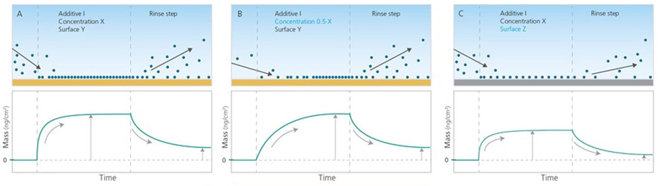
Chemical Mechanical Planarization (CMP), also referred to as Chemical Mechanical Polishing, combines chemical and mechanical processes to planarize semiconductor components. CMP is critical for creating uniform interlayer dielectric and metal layers and ensures a smooth topography for photolithography and metallization steps. A good understanding of the chemistry and surface interactions involved in CMP enables the optimization of CMP slurry formulations and process protocols for increased efficiency and better reliability and functionality of finished devices. Quartz Crystal Microbalance with Dissipation Monitoring (QCM-D) allows the simulation of CMP processes using relevant surface materials and chemicals to monitor how additives, additive mixtures, and abrasives interact with the surface of interest. Characterize slurry additive – surface interactions, study etching behavior of slurry formulas, analyze performance of cleaning agents for post-CMP residue removal, and uncover the interactions involved in CMP processes at the nanoscale with QCM-D analysis.
Schematic illustration (not to scale) of how the performance and behavior of CMP slurry additives can be compared using QCM-D
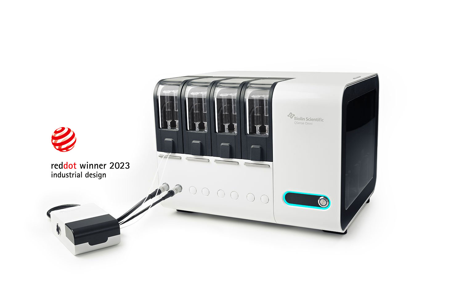
The QSense Omni QCM-D provides unparalleled, nanoscale sensitivity for real-time investigation and quantification of molecular interactions, mass changes, and viscoelastic properties at surfaces and interfaces. Simulate CMP systems with a wide range of available sensor surfaces, including: Cu, Co, W, Al, Sn, Si, SiO2, Si3N4, SiC, TEOS, polySi, Al2O3, CuO, SnO2, NiP, polyimide, and many more.