Table of Contents
What is Ion Milling?
Ion polishing and milling is a materials processing technique used to remove material from a sample surface by bombarding it with a beam of charged nuclei. The process relies on sputtering, in which energized ions physically eject other atoms and molecules from the sample surface through momentum transfer. Ion milling is commonly used in materials science and engineering for applications such as cross-sectioning samples, thinning samples for electron transparency, and removing layers for deeper analysis. The technique is an important tool for preparing specimens and revealing internal structures and compositions for investigation under electron microscopes.
There are two directions with sample preparation with ions: focused ion beam (FIB) and the near parallel ion technique (generally referred to as ion milling), with the key differences lying in the ion beam parameters. In the case of FIB, a finely focused beam of high energy ions (commonly gallium up to 30 keV) is used for precision milling in spot sizes of 50 x 50 μm, and preparing samples may take a significant amount of time.
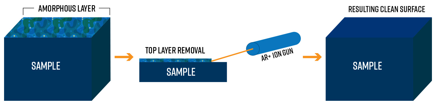
In contrast, the near parallel ion milling technique (show in Figure 1) involves energies less than 20 keV, and an inert gas such as argon is ionized and accelerated to form a broad, non-focused beam of ions which interacts with the sample surface. The kinetic energy of the incoming ions is converted to heat and momentum upon impact, breaking atomic bonds and ejecting material to remove thin layers in a controlled fashion. By rastering the ion beam across an area of interest, the exposed surface can be precision milled to a desired depth. Ion sources, beam optics, and sample manipulation stages have improved over decades of use, increasing the amount of control over parameters such as milling rate, resolution, and general surface finish.
Ion milling is valuable for materials science and microscopy applications where non-destructive slice and view investigation of internal sample features is required. When paired with scanning electron microscopy (SEM) or transmission electron microscopy (TEM) – and these are quintessential applications of ion milling – meticulously prepared cross-sectional samples enable detailed imaging and analysis of buried interfaces, compositional gradients, and defects below the surface of a whole range of materials [1].

Why use Ion Milling?
High resolution imaging of materials with techniques like scanning electron microscopy is critical for understanding the relationships between underlying structures that govern macroscopic properties. Due to this importance, proper sample preparation is one of the most vital components of the analysis process; however, it comes with a level of delicacy in that the process can often introduce amorphous layers or damaging defects which obscure features of interest. Mechanical polishing, the act of physical abrasion through methods like grinding with abrasive paper or sanding, induces deformation, scratches, and amorphous layers that distort the pristine material underneath. Chemical etching is a process that makes use of acidic or alkaline solutions for removing material, but it fails to provide a sufficient level of precision and control necessary for uniformity and applications in microscopy. Regardless of the exact method, preparation artifacts from polishing and etching can entirely mask critical aspects of sample microstructures [2]. Therefore, being able to eliminate the damaged layers to expose the original surface is vital. This is where ion milling has proven to be an invaluable technique.
Principles of Ion Milling
Ion milling material removal is fundamentally based on the sputtering process, whereby ion beam irradiation ejects atoms and clusters from a solid target. As energized ions collide with surface atoms, they transfer energy and impart momentum to the target material. Given sufficient energy transfer, this can break atomic bonds and dislodge particles from the underlying lattice. Gradually accumulated damage cascades from the beam erode the surface one layer at a time as ions penetrate below and disrupt interatomic forces.
The momentum and energy transfer between the incident ions and target material depends on factors such as the ion mass, ion energy, and binding energy of atoms in the target. Heavier ions like argon transfer more momentum, increasing sputter yields compared to lighter ions. However, lighter ions like helium penetrate deeper below the surface due to reduced scattering. Ion energy can be adjusted from a few hundred electron volts up to tens of thousands of electron volts to control milling rates and fit a particular application. Materials with lower atomic binding energies sputter more readily under ion bombardment.
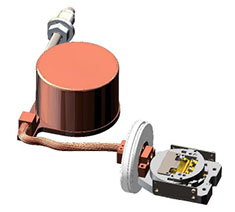
Ion Sources
Several ion source designs are commonly used in ion milling instruments, each with unique characteristics. To generate the required ion flux, source gases are ionized and accelerated to form a directed beam – inert source gases like argon and oxygen are commonly used as the feedstock for milling applications. The source gas can be ionized via collisions with free electrons from a hot filament cathode, or through electromagnetic induction to create a plasma discharge.
Radio frequency (RF) inductively coupled plasma (ICP) sources couple electromagnetic energy into a low pressure gas to create a plasma discharge independent of electrode degradation. An alternating RF electromagnetic field induces oscillations and collisions that strip electrons from gas atoms or molecules. With high plasma densities, the resulting rich supply of cations can then be accelerated into a beam.
Duoplasmatrons utilize a hot filament cathode to emit electrons that ionize gas molecules (such as those of argon) introduced into the vacuum chamber. The resulting plasma gets accelerated through dual positively charged anode grids, emerging as a directed ion beam. Duoplasmatrons feature modest beam intensities but simpler operation and lower costs compared to alternatives.
End-Hall ion sources – independent of any grids – rely on a closed drift architecture with crossed electric and magnetic fields. An applied voltage generates an axial current in the presence of a radial magnetic field, creating a concentrated plasma near the anode aperture that gets extracted as an intense ion beam.
Meanwhile, Freeman and Kaufman style hot cathode sources rely on electron emission from a heated filament, often thoriated tungsten, to initiate the ionization process in close proximity to an anode aperture [3]. In either case, the discharge produces a mixture of ions and electrons to subsequently source and focus with gridded extraction optics.
Cooling Options
Ion milling can induce significant heating of samples during prolonged irradiation. Managing thermal loads is critical to prevent undesired material changes and maintain precise control. Common cooling methods include:
Peltier thermoelectric cooling
Peltier modules utilize the thermoelectric effect to pump heat from one ceramic metal junction to another when an electric current is applied across two different semiconductor materials. This solid state heat flux enables precise temperature control suitable for ion milling samples.
Liquid nitrogen (LN2) cooling
Circulating or dripping liquid nitrogen onto the sample and stage provides a chilling effect through direct contact and evaporation. Temperature reductions between 100 degrees Celsius are feasible, though care must be taken to avoid moisture condensation and material embrittlement because the cold temperatures can make some samples fragile.
Electromagnetic lenses, deflectors, and quadrupoles collimate in the expanding plume into a beam. Charge to mass ratio guides the sorting of ion species based on their trajectories in applied fields. Heavier inert gas ions like argon reduce scattering effects and enable deeper penetration during milling. Lighter ions conversely allow for finer surface polishing. Thus the selected ion type and source conditions may cater to the particular sputtering requirements of a user.
By artful manipulation of electromagnetic fields, ion milling systems direct a well-formed beam toward any targeted sample area. Careful control over excitation parameters and beam optics unlocks the full potential of the sputtering process for the precise removal of materials.
What is the Ion Milling Process?
The ion milling process demands careful attention in sample preparation, instrumentation setup, and parameter selection to achieve controlled, artifact-free material removal.
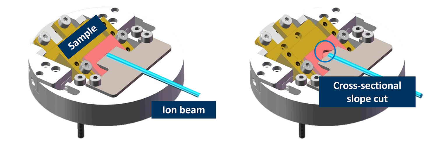
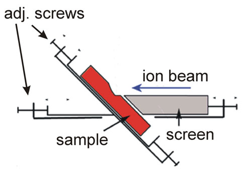
As a first step, mounting the specimen is critical to provide a solid base geometry and enable charge dissipation during milling. Adhesives like carbon tape fix the sample to a standard stub, with consideration for sample size, shape, and conductivity. Precise orientation is likewise imperative so that the ion beam accurately targets the region of interest. Without proper mounting and positioning, the beam could mill away unintentional areas or redeposit sputtered material across the target surface.
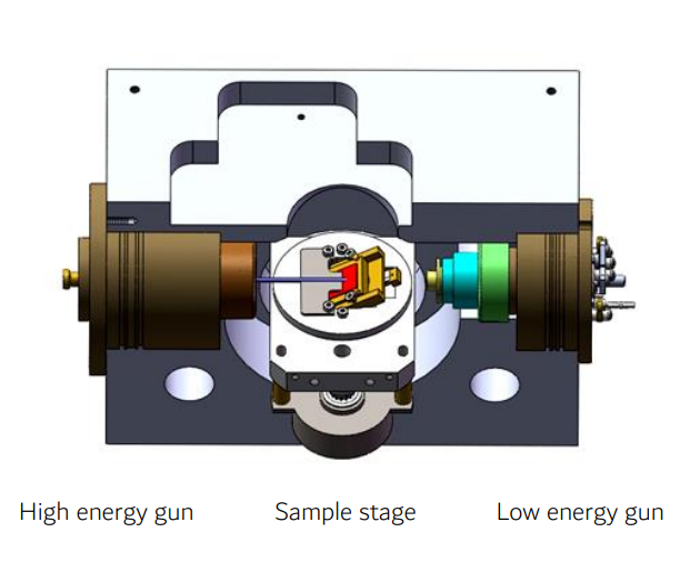
Electromagnetic lenses collimate the expanding ion stream into a cohesive beam directed toward the target. Deflector plates or scanning coils in the machine raster the ions over a defined area for uniform coverage. As for the beam energy, the range from hundreds to thousands of electronvolts suits different material removal requirements, though higher energies increase milling yield and depth that enable rapid bulk material removal. In addition, lower energies provide finer control for final polishing steps.
Sample Tilt
In SEM applications, sample manipulation stages tilt, rotate, and translate the specimen to adapt to milling geometries. Adjusting title angle controls the beam’s angle of incidence, which directly affects sputtering behavior: glancing angles yield slower material removal, while nearer-normal incidence increases yields.
Rotation during milling averages out angle effects for uniformity, whereas translation or oscillation enables cutting sloped surfaces.
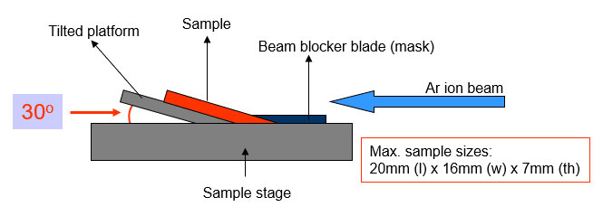
Slope cutting (creating new surface)
Slope cutting refers to the preparation of angled cross sections on samples using ion milling. This reveals internal structures for analysis and imaging of subsurface features. To cut a slope, the ion beam is typically directed at glancing incidence along the desired plane. The angle between the beam and sample surface helps control the overall slope angle, where shallower angles result in more gradual slopes. Typical shallow slopes are in the range of 15-30° but >45° slopes are also possible.
Tilting and rotating the sample stage during milling modifies the effective angle of incidence across the surface. For a consistent slope angle, the milling rate must be uniform across the target area. Parameters like beam current density, raster pattern, and scan speed all require optimization.
Applications of Ion Milling
Ion milling is an important sample preparation technique for material analysis using SEM and TEM. By precisely removing material from the surface, internal features (but what features can be exposed?) can be exposed for imaging and composition mapping.
EBSD
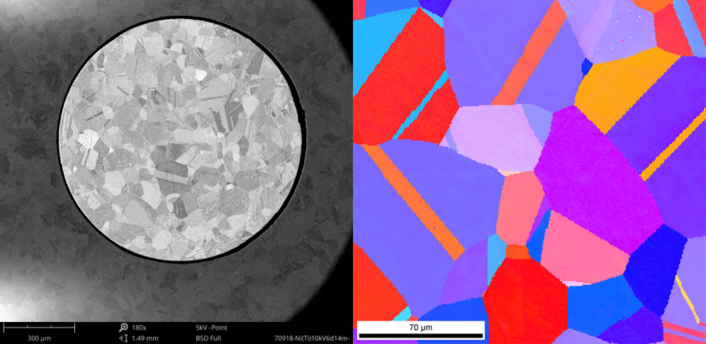
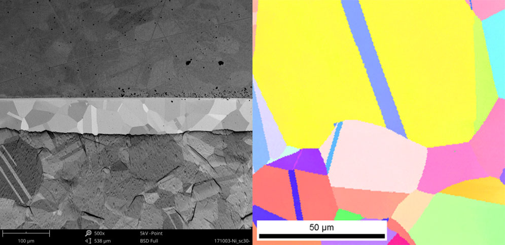
Electron backscatter diffraction (EBSD) is a microscopy technique used to study crystallographic structure and orientation in materials. An electron beam interacts with a tilted, polished sample and the resulting backscattered electrons form diffraction patterns that reveal information about the crystal structure, phase, orientation, and even strain state. However, for high quality EBSD analysis, the sample surface must be free of deformation and damage, which is exactly where ion milling excels.
With a pristine surface prepared by ion milling, EBSD can then construct orientation maps, misorientation profiles, grain size distributions, and phase identifications without artifacts obscuring the fundamental structure. Even minute changes in lattice distortion and orientation, indicative of residual stress fields, can be detected. The combination of ion milling sample preparation and EBSD analysis provides an incredibly powerful means to decipher texture development, recrystallization, alloy properties, and more in both engineered and natural materials [4]. Ion milling essentially unlocks the full potential of EBSD by removing the upper layers damaged during polishing to reveal the true crystallographic details in their unmodified forms.
SEM and TEM Across Industries
A major general application is cross-sectioning samples to reveal buried interfaces and structures. The ion beam can mill away layers parallel to the surface to create a clean cross-sectional face through the depth of a multilayered samples. This allows SEM imaging of internal interfaces between coatings, films, or composite materials that would otherwise be hidden. Elemental mapping by energy dispersive X-ray spectroscopy (EDS) can reveal diffusion profiles and compositional gradients.
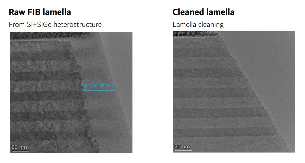
Ion milling is also indispensable for thinning down various samples and removing material to make them electron transparent for TEM analysis. The technique can mill samples down to a thickness of tens of nanometers so that electrons can transmit through the sample and interact to form an image. Thinning also reduces scattering and charging artifacts. TEM examination of focused ion beam prepared lamellas often utilizes ion milling as a final polishing step.
In terms of industries, ion milling is utilized across a diverse range of sectors due to its versatility as a precision material removal and sample preparation technique. Some of these are:
- Semiconductor Manufacturing: Ion milling is used to precisely etch or mill semiconductor wafers during device fabrication and processing. It can remove layers in an extremely controlled fashion.
- Surface Studies of Battery Electrodes: Milling battery electrodes exposes fresh surface layers for analysis by spectroscopy and other surface techniques. This gives not only morphological data, but chemical and electronic structure information on reactive surfaces in batteries as well.
- Removing Layers for Failure Analysis: Ion milling can be used to systematically remove material layers to expose and isolate the source of defects or failures for root cause analysis.
- Geology and mining: Intact cross sections of mineral samples is essential for viewing their internal structures. Because mechanical methods like sawing or polishing often damage crystalline structures and phase relationships in complex rocks and ores, ion milling stands as an ideal method to interpret rock origins and history.
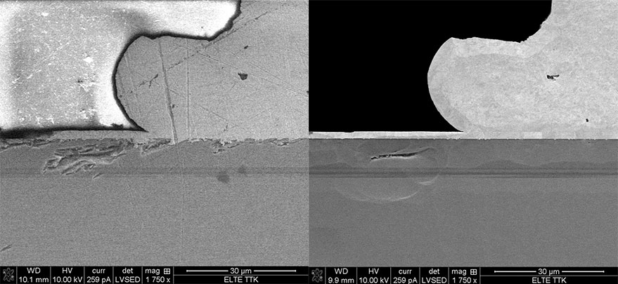
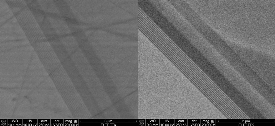
SEM images of a polished LED cross section (gallium nitride layers) comparing pre and post ion milling. As evidenced by the uniformity of the post images, mechanical polishing alone left unwanted amorphous layers which obscured the surface below.
Ion milling continues to support many applications in materials science, physics, and engineering research where invasive analysis and visualization of subsurface microstructures or compositions is needed. The technique provides a versatile materials removal method complementary to numerous other sample preparation tools.
References
[1] Howitt, D.G. (1984), Ion milling of materials science specimens for electron microscopy: A review. J. Elec. Microsc. Tech., 1: 405-414. https://doi.org/10.1002/jemt.1060010409.
[2] Ayodele, A. (2023, May 11). Ion Milling: A Comprehensive Guide to Material Etching Techniques. Retrieved from https://www.wevolver.com/article/ion-milling-a-comprehensive-guide-to-material-etching-techniques.
[3] Stephen E. Sampayan, Monroe L. King, Larry E. Frisa, Robert A. Moore, Jerald P. Dykstra, Enhanced ionization freeman ion source, Nuclear Instruments and Methods in Physics Research Section B: Beam Interactions with Materials and Atoms, Volumes 37–38, 1989, Pages 90-93, ISSN 0168-583X. https://doi.org/10.1016/0168-583X(89)90141-9.
[4] Nowak WJ. The Use of Ion Milling for Surface Preparation for EBSD Analysis. Materials (Basel). 2021 Jul 16;14(14):3970. doi: 10.3390/ma14143970. PMID: 34300889; PMCID: PMC8304033.