Scanning electron microscopy (SEM) is an incredibly adaptable analytical method that generates high-resolution images by scanning a focused electron beam across the surface of a sample. Inside the SEM instrument, a range of detectors captures various signals produced during the interaction between the electron beam and the sample, enabling the visualization of surface microstructure and elemental composition. Compared to optical microscopes, the exceptional resolving capacity of SEMs establishes them as an essential instrument across numerous industries, particularly those working with functional materials.
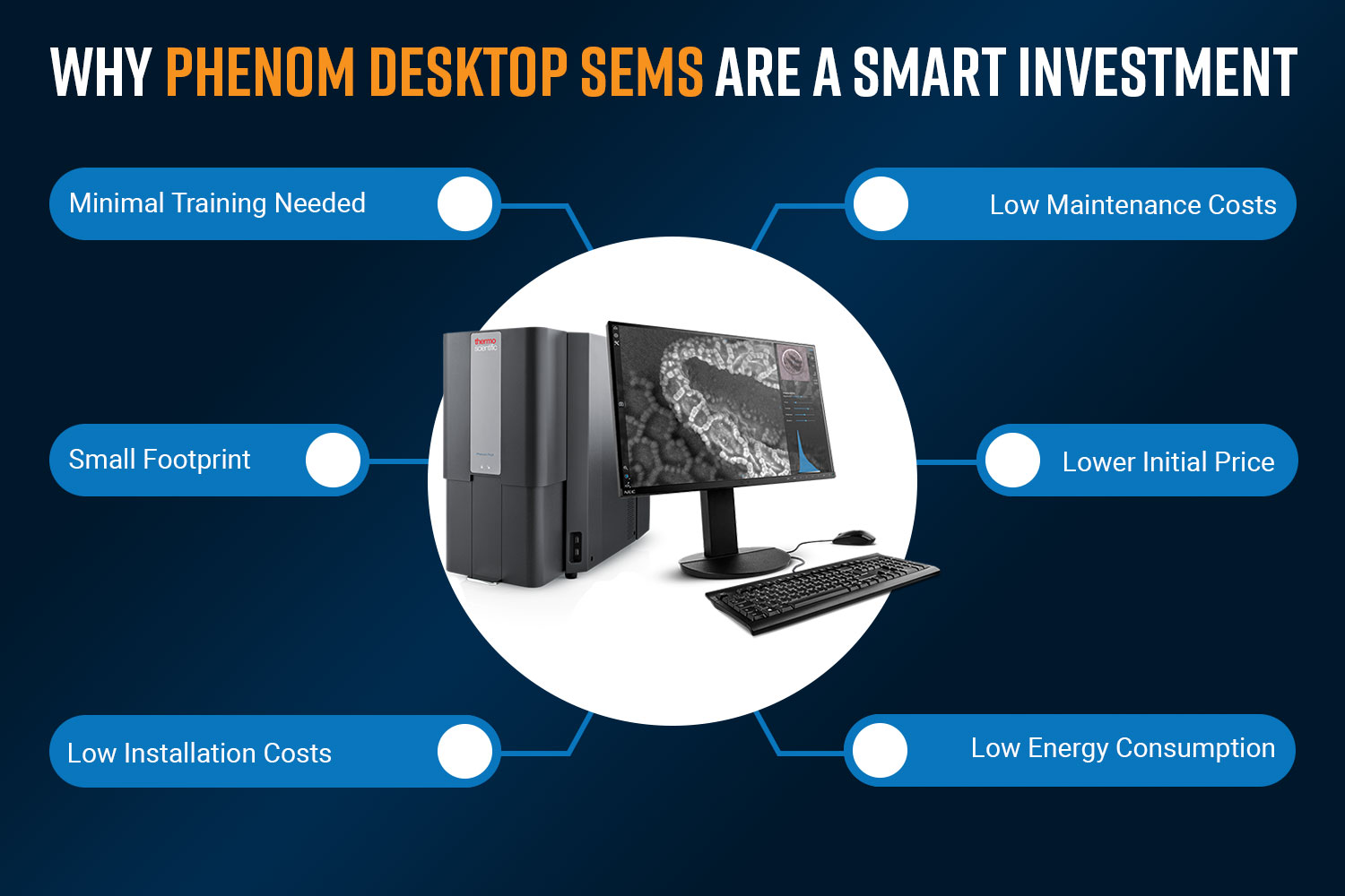
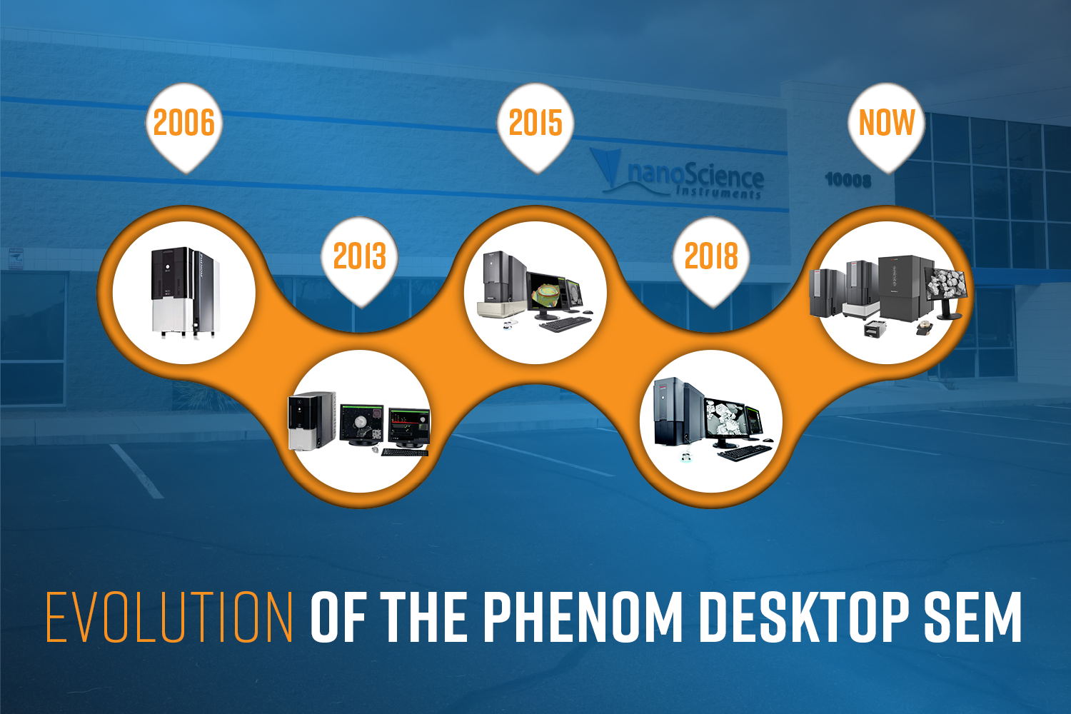
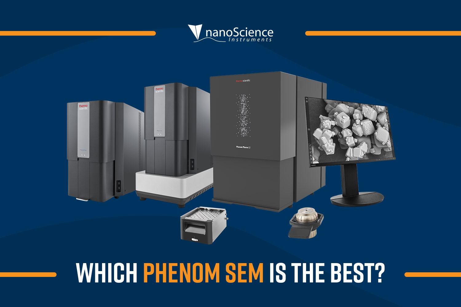
Many institutions are contemplating the incorporation of desktop SEM into their resources, aiming to enhance accessibility, reduce expenses, and accelerate data acquisition. Due to a combination of factors, Phenom Desktop SEMs have garnered a reputation as the best-selling models in the desktop SEM market. Their exceptional imaging capabilities, user-friendly interface, and compact design offer a seamless experience for researchers and professionals alike. The full lineup offers varying levels of capabilities in terms of resolution, magnification range, sample size, detectors, and electron sources. Understanding which Phenom best fits your needs will ensure you make a worthwhile investment now and in the future.

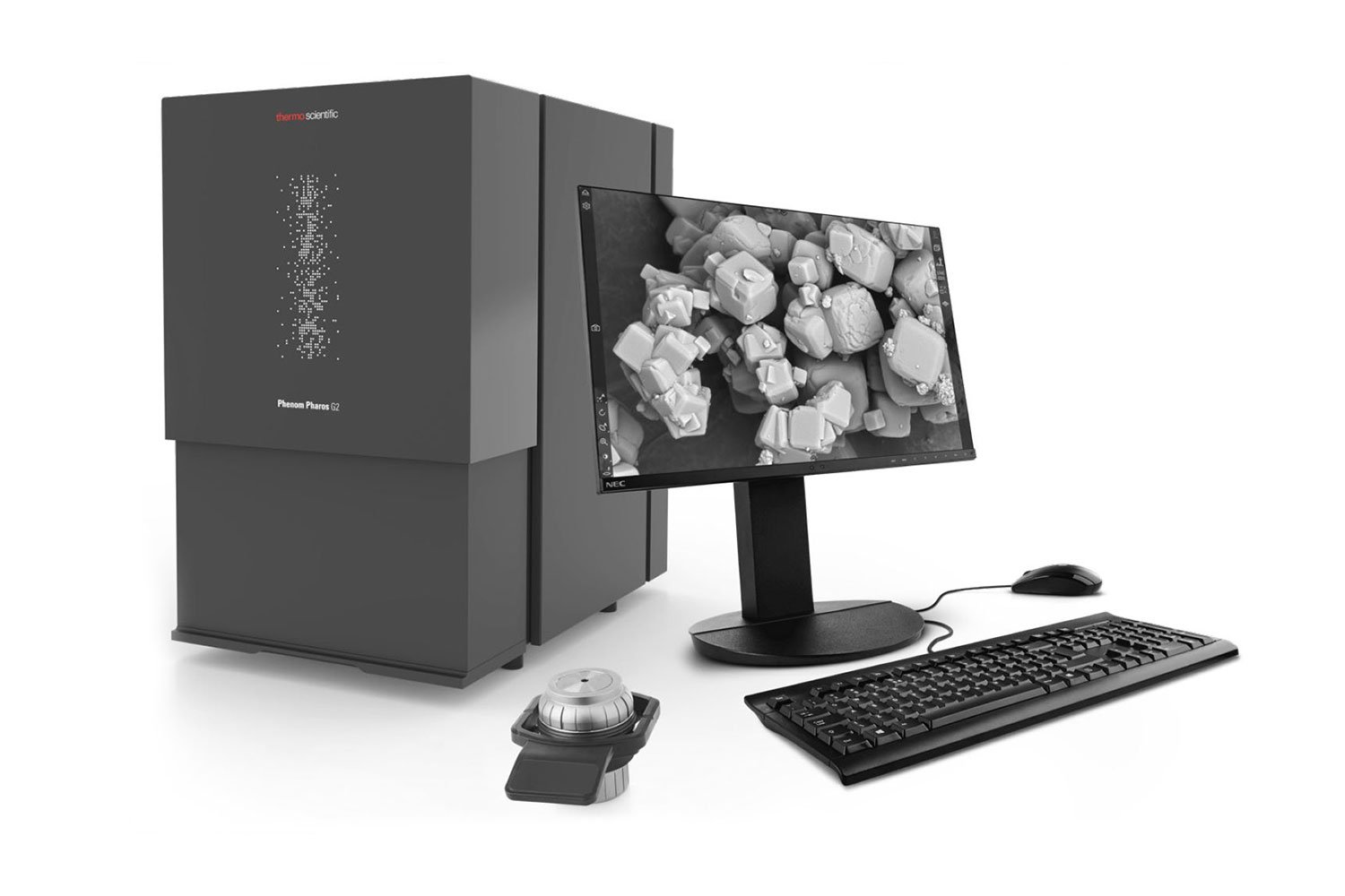
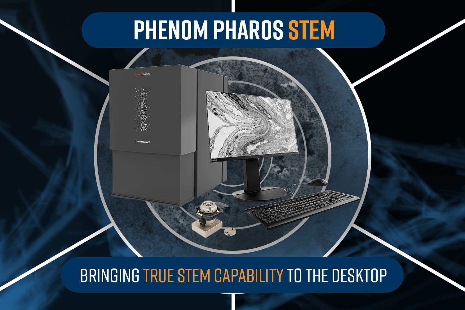
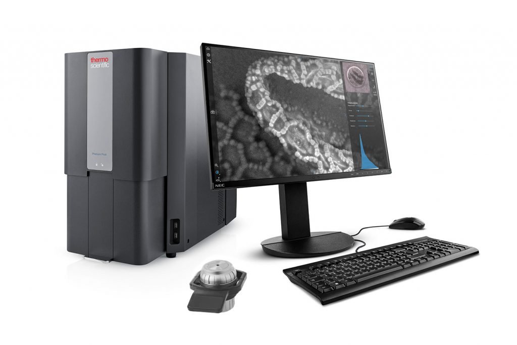
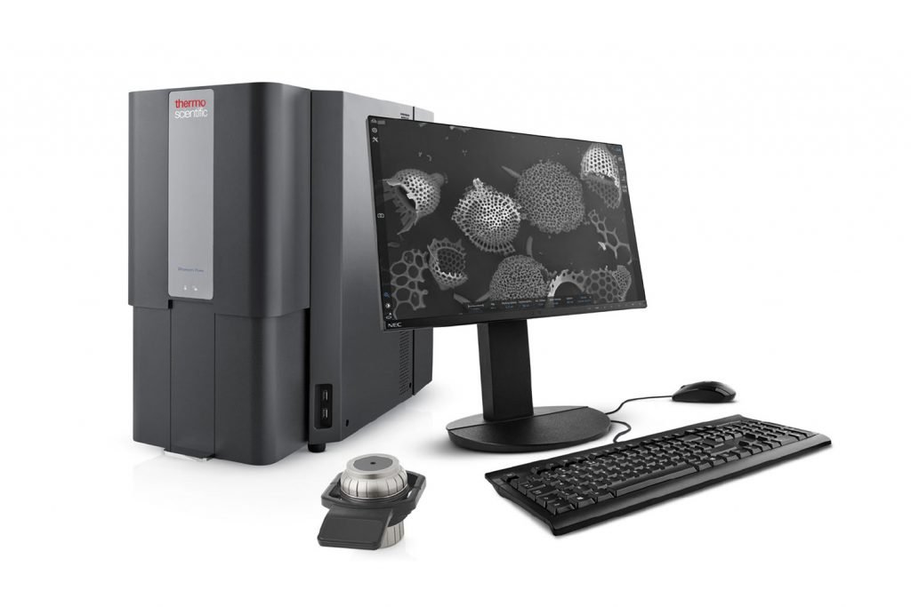
Phenom Pharos:
The Phenom Pharos stands out as the most advanced desktop SEM, boasting a field emission gun (FEG) making it excel at applications that demand high spatial resolution and low kV imaging capabilities. It can reach magnifications up to 2,000,000x and provides the highest resolution of any other desktop SEM on the market. Another exclusive feature of the Pharos is the ability to seamlessly switch between SEM and STEM imaging modes simply by inserting the Phenom Pharos STEM Holder. It provides three standard transmission imaging modes at a resolution of <1 nm, providing an unprecedented opportunity for fast and accessible STEM imaging for many applications.
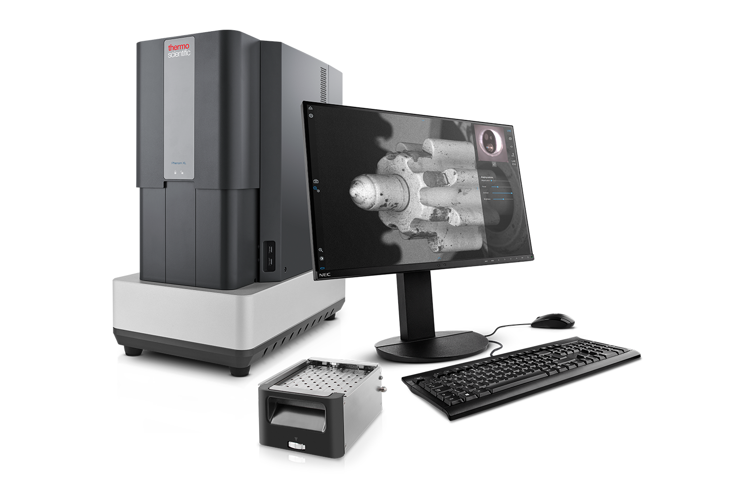
Phenom XL:
The Phenom XL boasts the most extensive sample capacity, accommodating a diverse range of specimens, from numerous small items to a singular bulk mass, to anything in between. The Phenom XL can accommodate samples as large as 100 x 100 mm or as many as 36 pin stubs. It comes standard with a segmented backscatter electron detector (BSD) and can be upgraded with a secondary electron detector (SED) and energy-dispersive X-ray spectroscopy (EDS) detector. The XL pushes the boundaries of desktop SEM with automation. ParticleX software enables end-to-end data collection and analysis for the Phenom XL with several ready-to-use packages and endless workflow customization.
Phenom Pro/ProX:
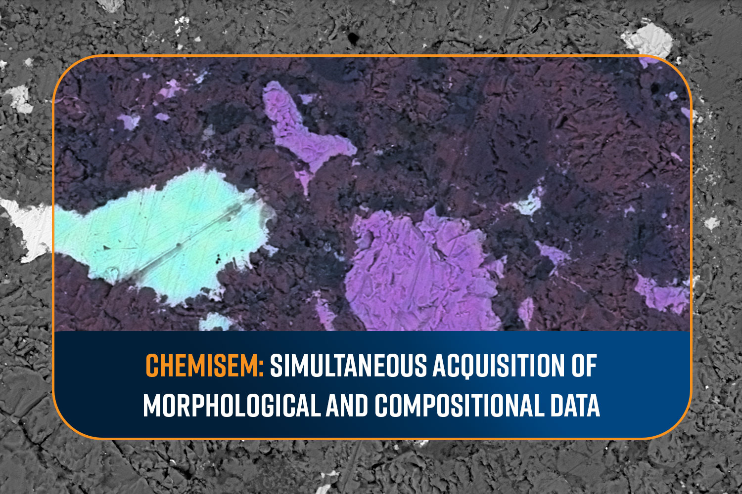
The Phenom Pro provides high-performance SEM imaging with enhanced resolution. Offering a continuous range of accelerating voltages from 5 kV up to 20 kV enables flexibility for analyzing a variety of samples. It comes standard with a BSD and is equipped with powerful yet intuitive software to allow for seamless operation for both new and experienced users. Adding a SED is also available as an option. The Phenom Pro can be upgraded to a Phenom ProX with the addition and an EDS detector to expand its capabilities. With the addition of the EDS detector and elemental analysis software, the ProX offers an all-in-one platform for high-resolution microstructural and compositional analysis.
Phenom Pure:
The Phenom Pure represents an affordable, desktop SEM that serves a variety of purposes. It finds utility in educational settings, basic research and development, as well as general imaging needs. Pure offers a simple yet effective imaging solution with two discrete accelerating voltages (5 or 10 kV), enabling the visualization of sample characteristics, surfaces, and structures. The Phenom Pure comes standard with a BSD and a SED is optional. An EDS detector can also be added to enhance the utility of Phenom Pure.
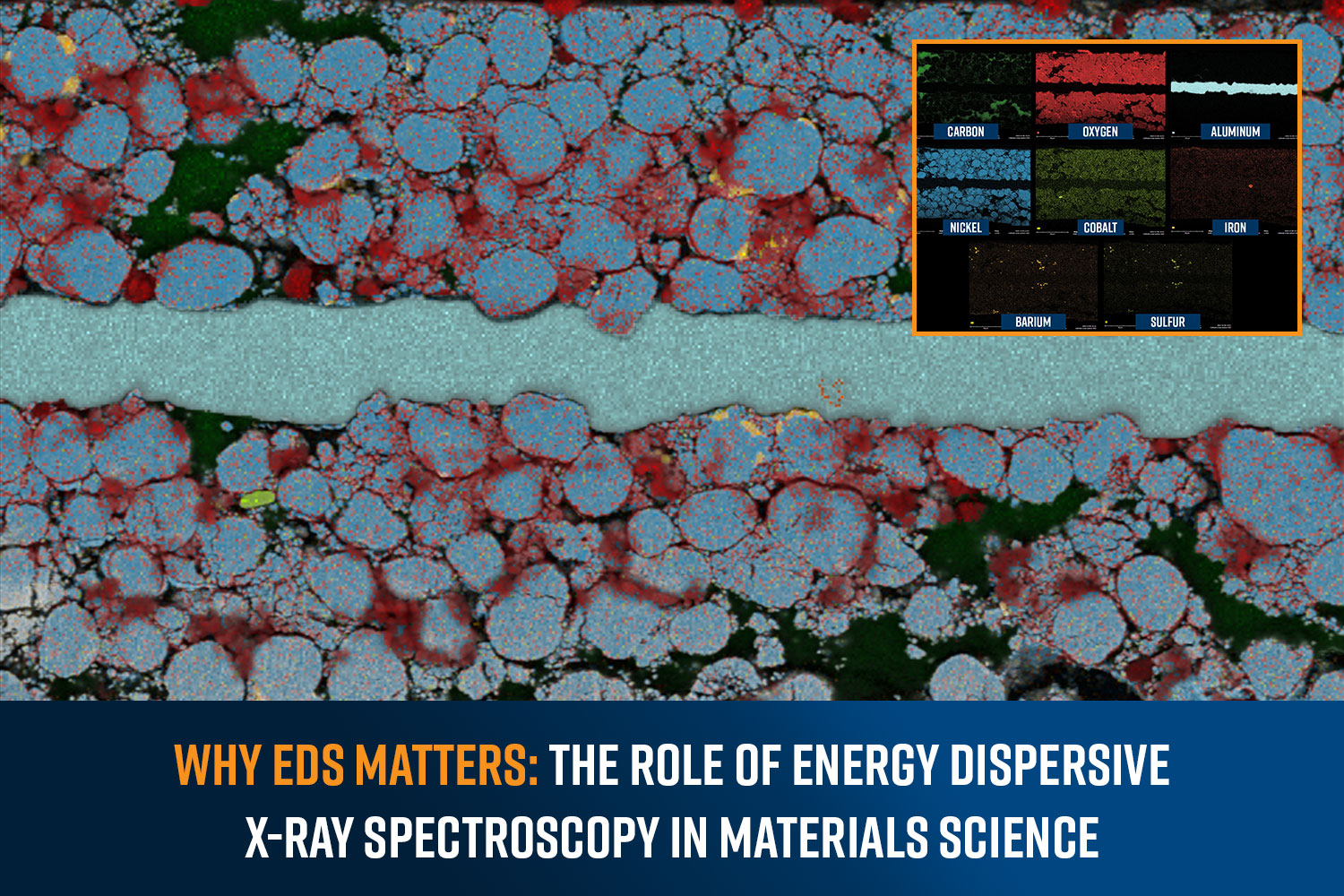
The Phenom XL, Phenom Pro, and Phenom Pure come standard with a CeB6 source that provides high X-ray count rates, greatly reducing the time-to-results compared to traditional tungsten-based systems. Combined with the seamlessly integrated silicon drift detector (SDD) for EDS, Phenom SEMs can detect elements spanning from Boron to Californium. Actionable data can be acquired in less than 60 seconds, even over large areas.
Compare all Phenom Models
| Phenom Pharos | Phenom XL | Phenom Pro/ProX | Phenom Pure | |
|---|---|---|---|---|
| Electron Source | Field Emission Gun (FEG) | CeB6 crystal | CeB6 crystal | CeB6 crystal |
| Max. SEM Magnification | 2,000,000x | 200,000x | 350,000x | 175,000x |
| SEM Resolution – BSD | 3 nm | 9 nm | 8 nm | 15 nm |
| SEM Resolution – SED | <2 nm | 9 nm | 6 nm | 15 nm |
| Acceleration Voltages | 1 – 20 kV | 1.5 – 20 kV | 1.5 – 20 kV | 2, 5 or 10 kV |
| Navigation Camera | ||||
| Sample Handling | Single pin stub 25 mm diameter |
Up to 36 pin stubs 100 mm x 100 mm |
Single pin stub 25 mm diameter |
Single pin stub 25 mm diameter |
| Detectors | BSD – Four-quadrant backscattered electron detector (standard) SED – Everhart-Thornley secondary electron detector (optional) EDS/EDX/EDAX – Integrated energy dispersive x-ray spectrometer (optional) |
|||
| STEM Mode | Optional | N/a | N/a | N/a |
Summary
All Phenom Desktop SEMs are built on a platform of resilient hardware and fully integrated software to deliver a best-in-class user experience at a minimal cost of ownership. Keep in mind that the choice of the specific configuration can greatly influence the results and efficiency of your research. Taking the time to evaluate the different capabilities and upgrade options will help you make a confident decision.