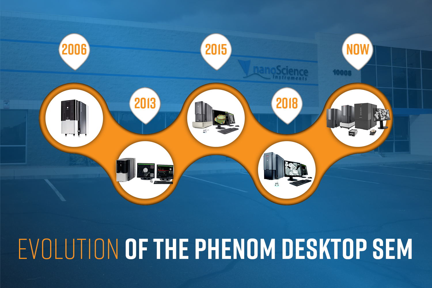
The Phenom Scanning Electron Microscope (SEM) is turning 20 this year! In celebration of this milestone, it is worth reflecting on how the platform has…
Posted: May 13, 2026 | Technology: Scanning Electron Microscopy
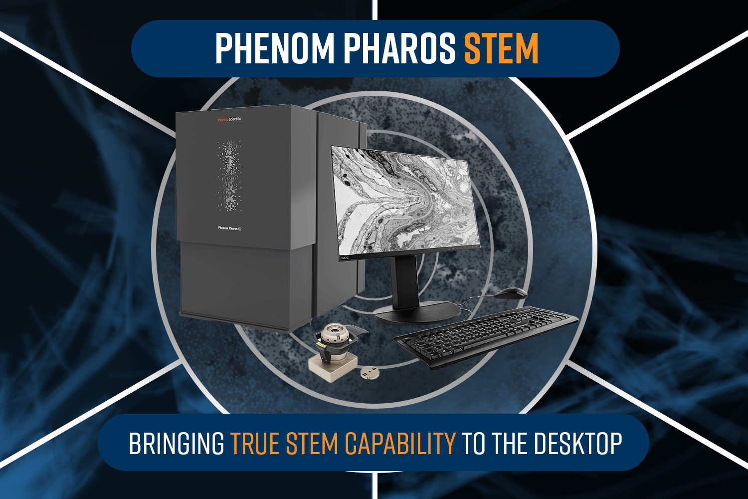
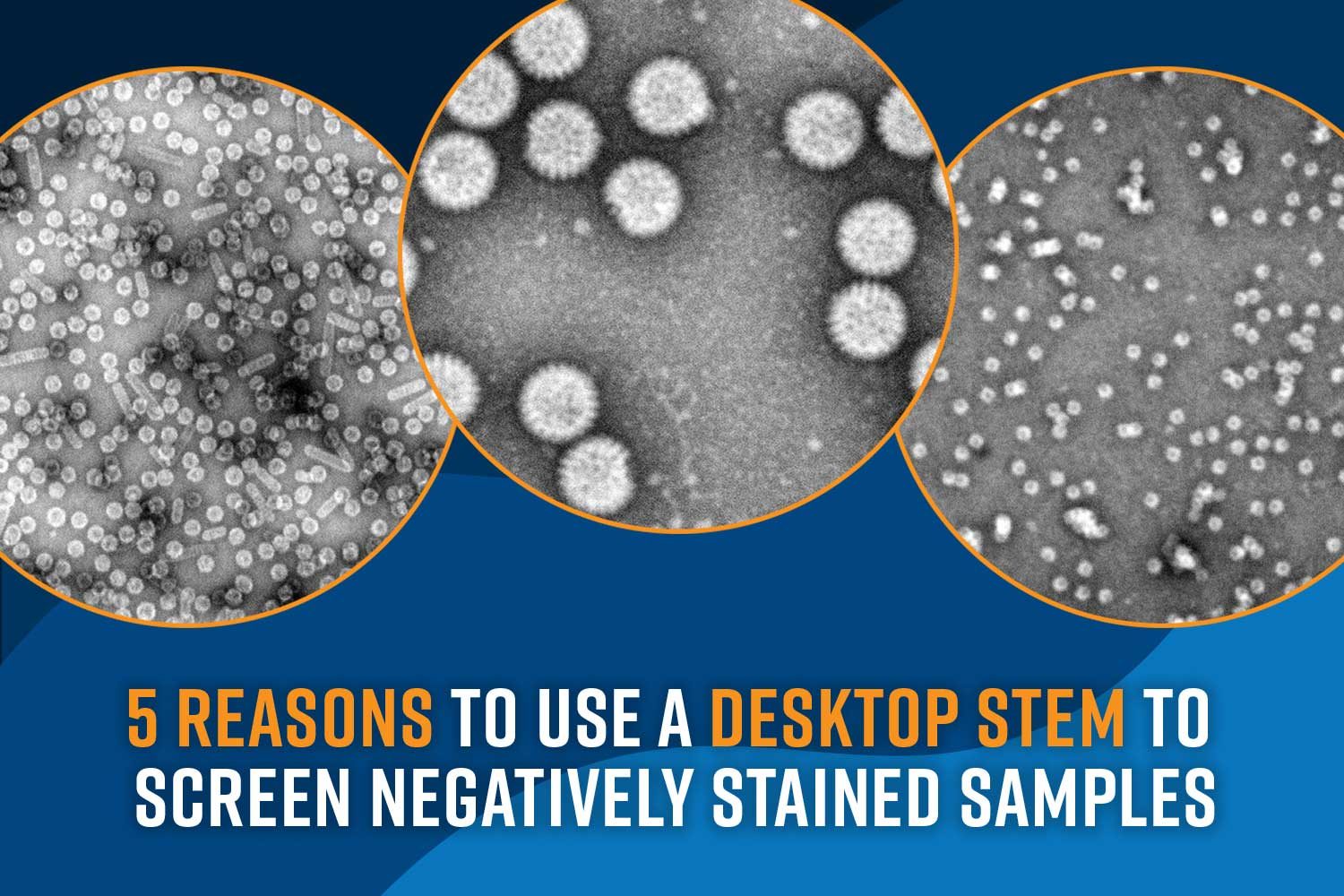
Scanning Transmission Electron Microscopy (STEM) is a scanning-based imaging technique that uses a focused electron beam to raster scan across an ultra-thin sample, typically <150…
Posted: April 29, 2026 | Technology: Scanning Electron Microscopy

When preparing samples for electron microscopy, the choice of method directly impacts the clarity and reliability of the images. Imperfections such as roughness, contamination, or…
Posted: October 15, 2025 | Technology: EM Sample Prep, Scanning Electron Microscopy
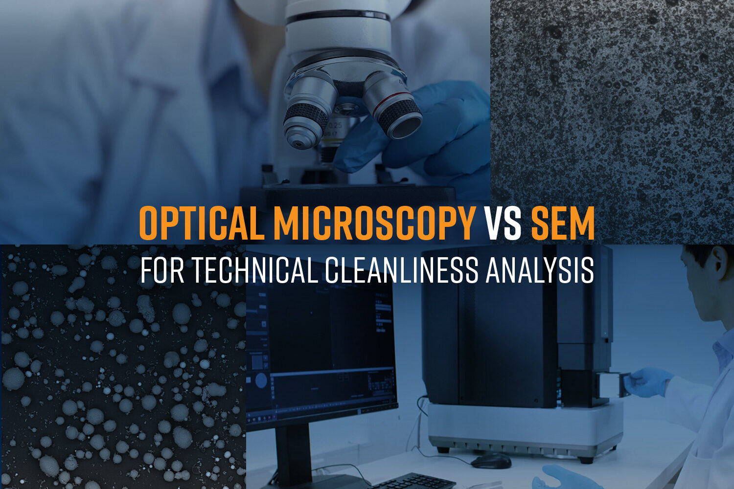
The performance of sensitive systems such as engines, hydraulics, electronics, and medical devices can be compromised in cases of particle contamination; this reduces product quality…
Posted: September 17, 2025 | Technology: Scanning Electron Microscopy
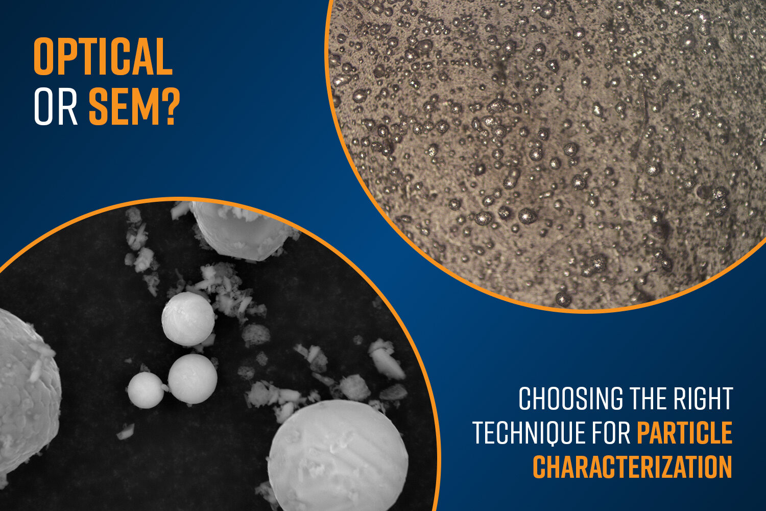
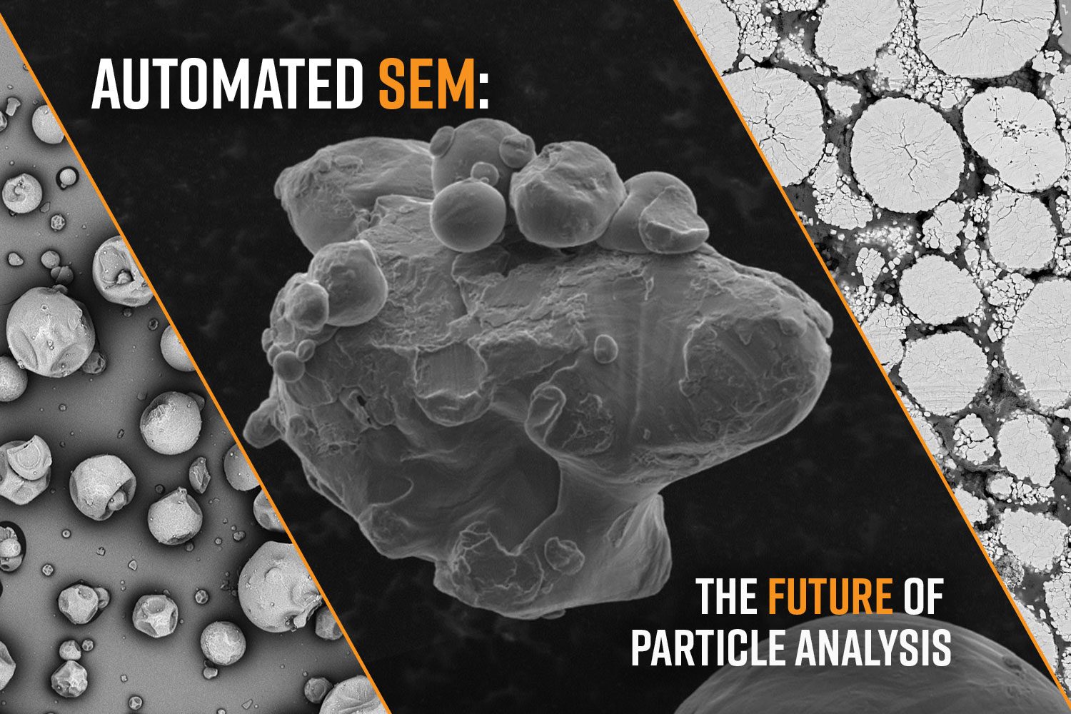
Particle analysis, which typically focuses on parameters such as size, shape, distribution, concentration, and composition, plays a critical role across a wide range of industries,…
Posted: September 3, 2025 | Technology: Scanning Electron Microscopy

What is Particle Analysis? Particle analysis is the measurement and characterization of particles in a sample. Particle analysis typically focuses on properties such as particle…
Posted: August 6, 2025 | Technology: Scanning Electron Microscopy
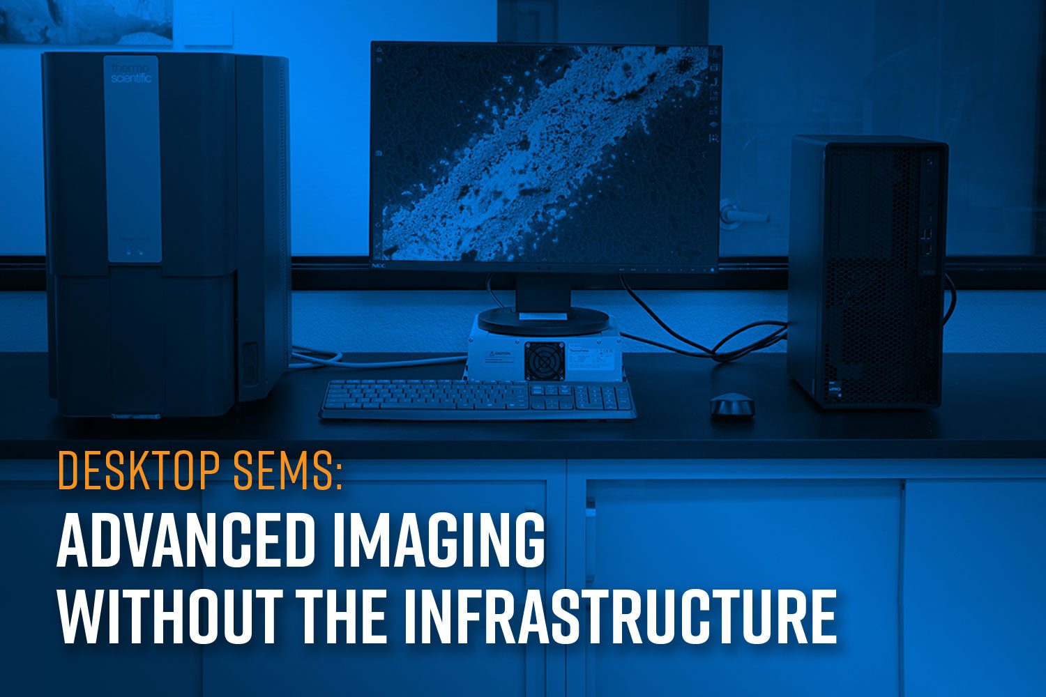
Scanning Electron Microscopes (SEMs) are indispensable tools for analyzing surface morphology, materials composition, and microstructural details at high resolution. They are used extensively across research…
Posted: July 23, 2025 | Technology: Scanning Electron Microscopy
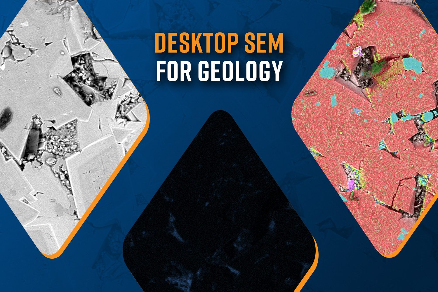
Scanning Electron Microscopy (SEM) is a versatile tool in geology used in high-resolution imaging and chemical analysis of rocks, minerals, and microfossils. SEM provides detailed…
Posted: May 7, 2025 | Technology: Scanning Electron Microscopy
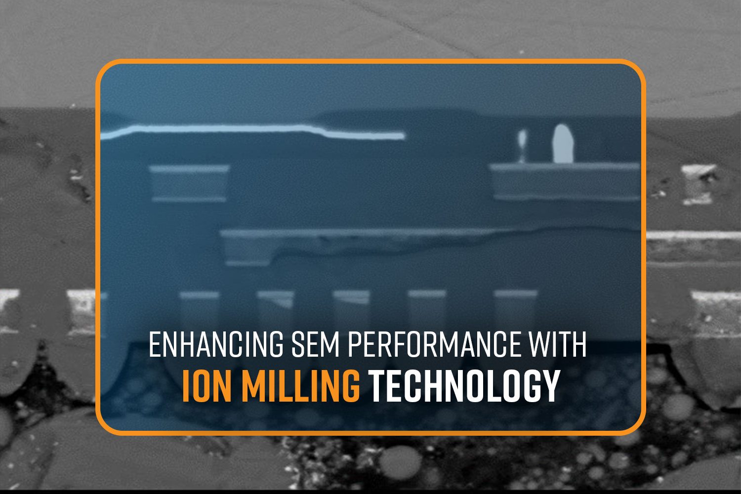
In material science, cross-section polishing is a critical method to enable the detailed examination of a sample material’s microstructure. This technique is essential for understanding…
Posted: April 30, 2025 | Technology: EM Sample Prep, Scanning Electron Microscopy
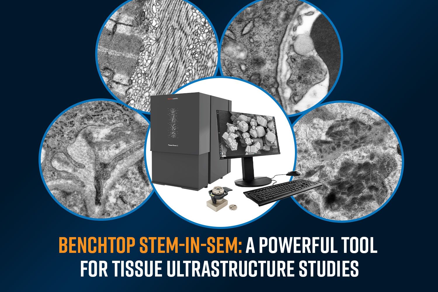
Understanding the ultrastructure of biological tissues is essential for advancing medical research, disease diagnostics, and drug development. Traditionally, histological techniques such as optical microscopy have…
Posted: April 23, 2025 | Technology: STEM, Scanning Electron Microscopy
Particle analysis involves characterizing the size, morphology, and composition of powders and particulate matter to describe their properties in a precise and statistically significant manner….
Posted: April 9, 2025 | Technology: Scanning Electron Microscopy
Cryo-electron microscopy (cryo-EM) is a powerful imaging technique used to determine the structure of biological macromolecules, viruses, and cellular components at near-atomic resolution. Unlike traditional…
Posted: March 26, 2025 | Technology: STEM, Scanning Electron Microscopy