In the age of climate change and resource depletion, the circular economy is increasingly gaining attention. It promotes the reuse, recycling, and repurposing of materials to create sustainable production and consumption systems. One essential tool that enables this process is Scanning Electron Microscopy (SEM), which provides detailed insights into the structural and compositional properties of recycled materials. SEM provides a powerful and accessible solution for detailed analysis of recycled material microstructures, surface characteristics, and elemental composition, making it an essential tool for both R&D and quality control in recycling industries.

The Role of SEM in Material Characterization
SEM is a powerful imaging technique that allows scientists to visualize materials at the micro- and nanoscale. By using a focused beam of electrons, SEM captures detailed images of a material’s surface, revealing key structural features such as texture, porosity, and defects. In addition to imaging, SEM can be coupled with Energy Dispersive X-ray Spectroscopy (EDS) to probe the distribution of elements within a material, offering insights into their composition, degradation, and potential contaminants.
SEM characterization helps evaluate the physical integrity and chemical makeup of recycled materials, ensuring they meet industry standards and are safe for reuse. This is particularly important for materials such as metals, plastics, and composites, which may undergo degradation or contamination during their lifecycle.
Why SEM Matters in Recycling Processes
One of the main challenges in the recycling industry is ensuring that recycled materials can match the performance and reliability of their virgin counterparts. SEM is a critical tool in overcoming this challenge. It helps:
Assess Material Degradation
Over time, materials degrade due to environmental exposure, mechanical stress, and chemical reactions. SEM can detect microcracks, fractures, and other imperfections in recycled materials, which are often invisible to the naked eye. These insights can guide further processing steps to improve the material’s durability.
Detect Contamination
Materials to be recycled often contain impurities or unwanted additives. SEM-EDS analysis can identify these contaminants at the elemental level, allowing for the refinement of recycling processes to remove or reduce them. This is particularly crucial in industries like electronics recycling, where toxic elements such as lead, or mercury may be present.
Optimize Recycling Methods
Understanding the microstructure of recycled materials through SEM can lead to more efficient recycling techniques. For example, in the case of polymers, SEM can reveal how well the material responds to different thermal or chemical treatments, helping to optimize processes for better quality outcomes.
Ensure Quality Control
The use of SEM allows manufacturers to develop strict quality control measures for recycled materials. By regularly examining the structural properties of materials during and after the recycling process, SEM ensures that only materials meeting specific standards are reintroduced into the production cycle.
Applications of SEM in Different Recycling Streams
SEM characterization is critical across various recycling streams including:
Plastic Recycling
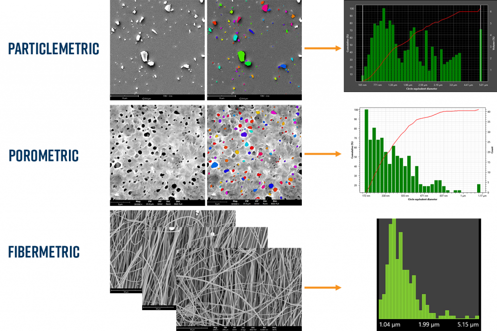
In the recycling process, plastic is sorted, cleaned, and transformed into pellets that serve as raw material for new products. SEM helps by detecting issues like surface defects, voids, and fiber orientation in the recycled material, as well as measuring the particle size of the input feedstock. Automated SEM image analysis solutions (Figure 1) allow recyclers to perform these analyses quickly and consistently, enabling them to make informed, data-driven decisions that improve the recycling process.
Metal Recycling
Recycling metals like aluminum, steel, and copper reduces the demand for raw material extraction. However, controlling impurities such as alloying elements or oxidation in recycled metals is essential to maintain their mechanical properties. SEM and EDS enable detailed metallurgical analysis at high magnifications, ensuring that recycled materials meet the necessary quality standards. Automated SEM-EDS solutions, like Phenom ParticleX Steel, quickly identify and analyze non-metallic inclusions, which can affect the metal’s strength and durability (Figure 2). This ensures recyclers can maintain high-quality standards in the final products.

Construction Materials
Recycling concrete, asphalt, and other construction materials is a growing area of focus. SEM imaging and image analysis allows for the detailed examination of pore structures, cracks, and interfacial zones in recycled aggregates (Figure 3).1 This helps engineers design better recycling protocols to ensure that construction materials maintain their structural performance when reused.
Electronic Waste (E-waste)
E-waste contains valuable metals and rare earth elements that can be recovered. SEM-EDS enables detailed mapping of the elemental composition within electronic components, such as circuit boards, connectors, and capacitors (Figure 4). This allows recyclers to precisely locate valuable metals, rare earth elements, and other recoverable materials at the microscale, facilitating targeted extraction.2 Electronic materials may also contain hazardous substances such as lead, mercury, or cadmium. With SEM and EDS, the location of these contaminants can be pinpointed which can help to inform safe handling and separation procedures.

The Path Forward: SEM and Circular Economy Innovation
As the world pushes toward a more sustainable future, SEM characterization will continue to play a pivotal role in advancing the circular economy. Its ability to provide in-depth, precise data about the physical and chemical properties of recycled materials helps bridge the gap between raw and recycled material performance. By enabling better quality control, contamination detection, and process optimization, SEM allows industries to confidently integrate recycled materials back into the supply chain, reducing reliance on finite resources.
Additionally, ongoing advancements in SEM technology are expected to further enhance its application in recycling. With the development of faster, more powerful microscopes, real-time monitoring of recycling processes may become possible, enabling more immediate and effective adjustments. This, in turn, will accelerate the adoption of sustainable practices across industries.
In conclusion, SEM characterization is more than just a technical tool; it is a catalyst for innovation within the circular economy. By ensuring the quality and safety of recycled materials, SEM supports the transition to a system where waste is minimized, and materials are continually repurposed, creating a sustainable and resilient future.
References
- M. J. Chinchillas-Chinchillas, C. A. Rosas-Casarez, S. P. Arredondo-Rea, J. M. Gómez-Soberón and R. Corral-Higuera, “SEM Image Analysis in Permeable Recycled Concretes with Silica Fume. A Quantitative Comparison of Porosity and the ITZ,” Materials, vol. 12, no. 13, 2019. https://doi.org/10.3390/ma12132201 ↩︎
- S. Brožová, M. Lisińska, M. Saternus, B. Gajda, G. S. Martynková and A. Slíva, “Hydrometallurgical Recycling Process for Mobile Phone Printed Circuit Boards Using Ozone,” Metals, vol. 11, no. 5, p. 820, 2021. https://doi.org/10.3390/met11050820 ↩︎

