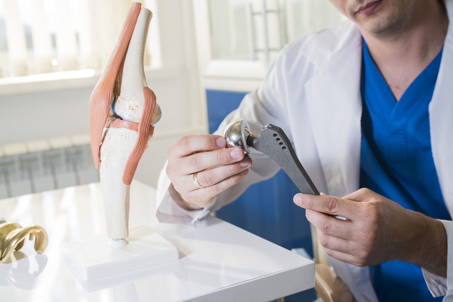
Implantable medical devices are continually pushing the boundaries of what is possible when modern medicine and engineering join forces. An implantable medical device is an instrument that is surgically inserted into a patient’s body to restore or enhance function to diseased or injured parts of the body. Common examples include pacemakers for correcting heart arrhythmia, artificial hip and knee joints, cardiac stents, and cochlear implants.
In this ever-evolving landscape, medical devices are being miniaturized to promote a minimally invasive approach thereby increasing their effectiveness and biocompatibility. Take for example implantable glucose monitors, which offer continuous and automatic monitoring to manage diabetes more effectively. Developing and manufacturing such devices comes with an ever-increasing need for precision processes with an eye on the micro- and nano-level. One technology that has revolutionized the way we examine, analyze, and improve medical devices is scanning electron microscopy (SEM). With its ability to provide high-resolution images and elemental maps, SEM has emerged as an indispensable tool for researchers and engineers in the field of medical device manufacturing.
Examples of how SEM is used in the Medical Device Industry:
In the field of medical devices, SEM has several essential applications:
1. Surface Characterization:
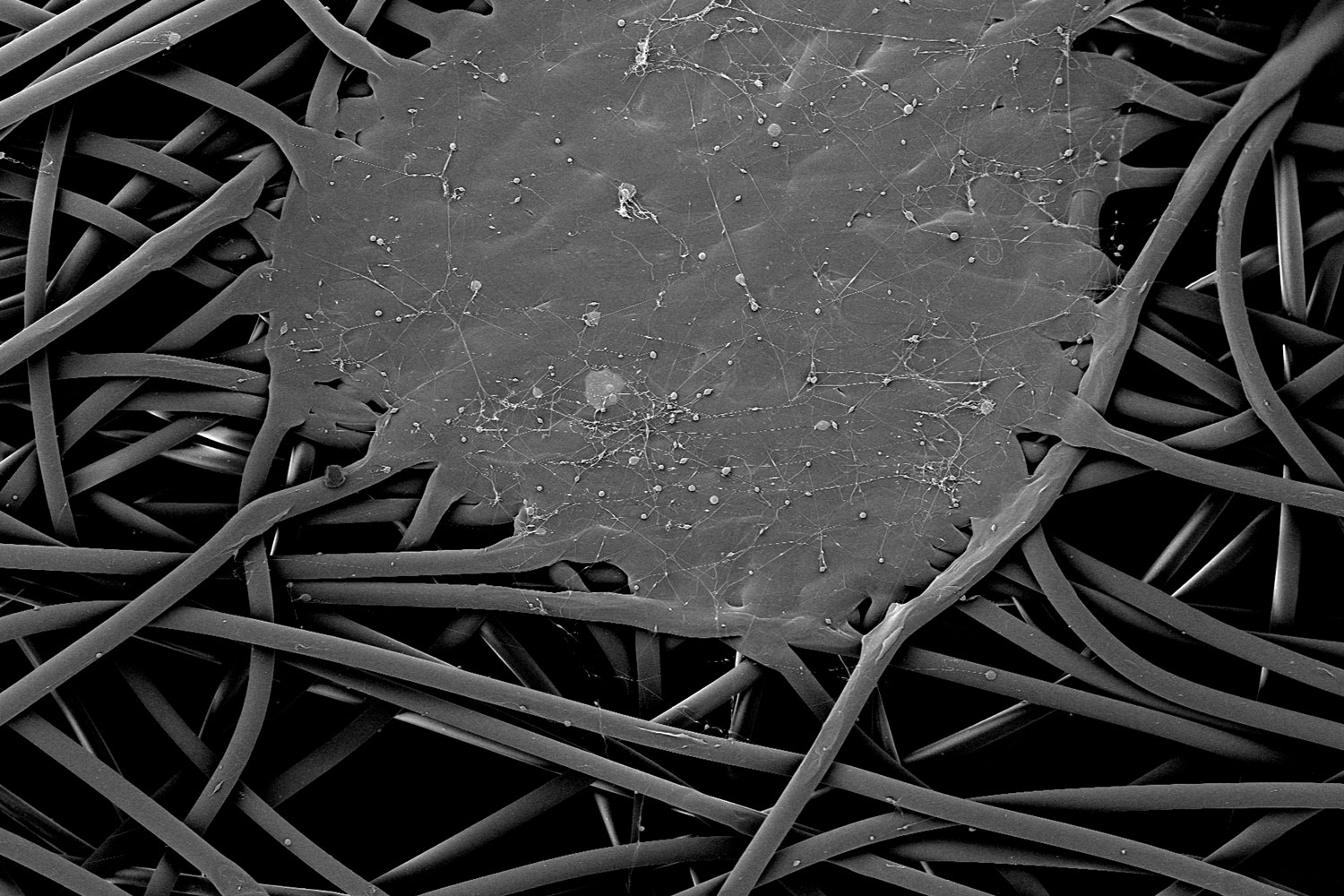
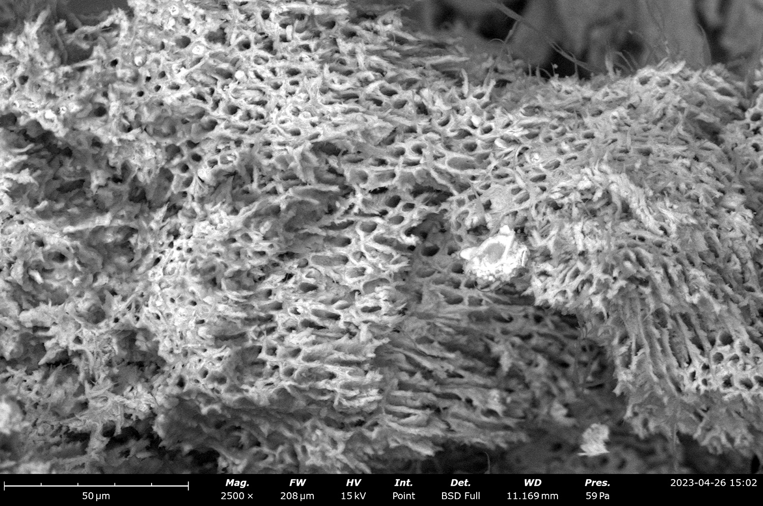
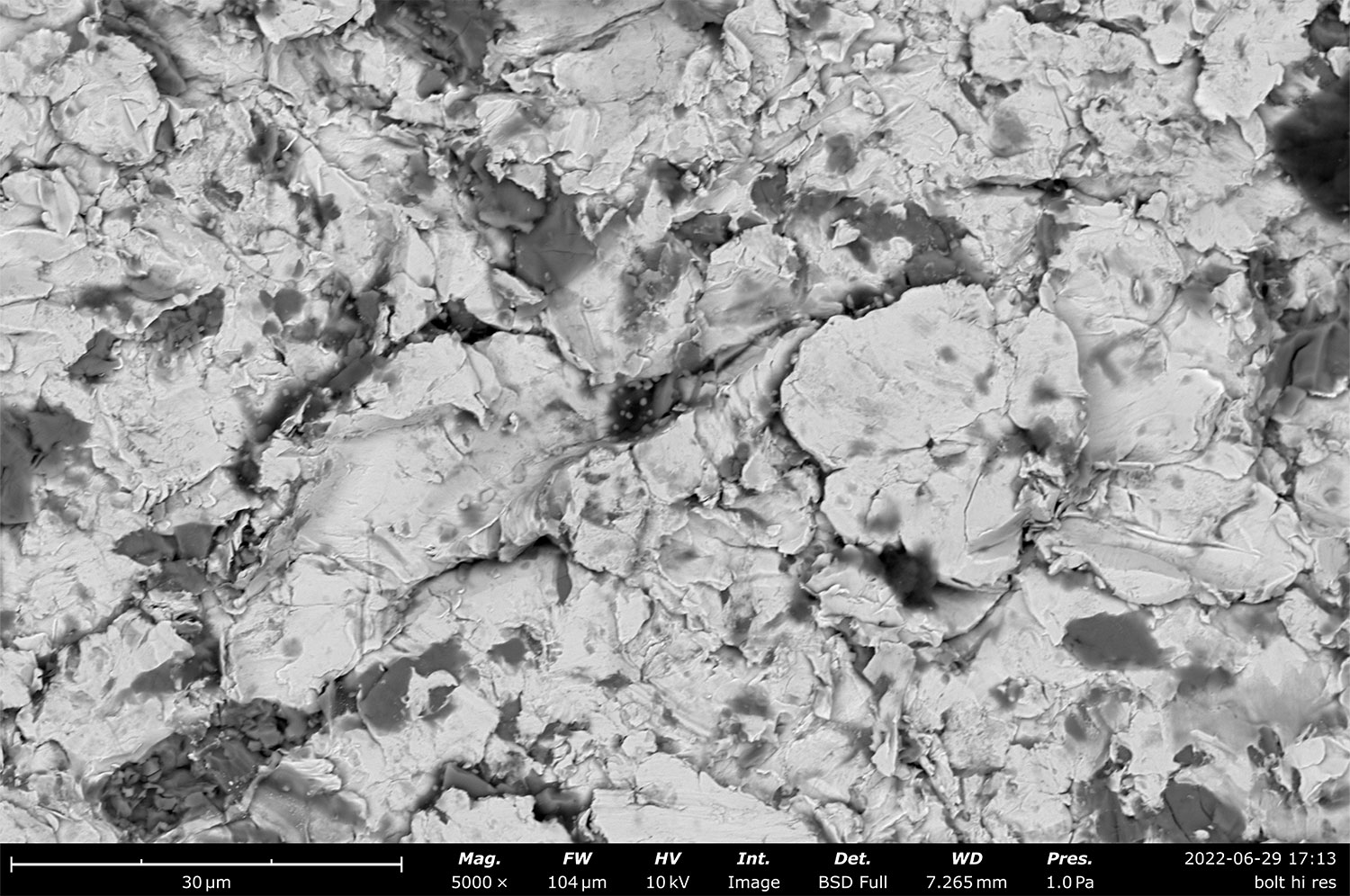
SEM can be used to examine the surface morphology, topography, and roughness of medical device materials. The backscattered electron detector (BSD) can be used to generate images with contrast sensitive to atomic number, making it useful for identifying different materials and phases that may be indicative of contamination. Segmented BSD detectors, in which the electron sensor is broken into four quadrants, can be leveraged to generate topographical images and three-dimensional roughness maps. This can be useful for further characterization of a defect or to compare the smoothness of an implantable device. On the other hand, secondary electron detector (SED) images produce images with surface topography contrast by collecting electrons that uniformly emanate from a shallow depth within the volume of interaction. SED images possess better spatial resolution compared to BSD images and provide complementary information thus allowing for comprehensive surface characterization.
2. Failure Analysis:
In the rare event that an implantable medical device fails in the field, the device will usually be sent back to the manufacturer to reverse engineer the failure. SEM is widely employed to investigate the root causes of device failures, defects, or malfunctions. It can reveal structural defects, fractures, wear patterns, and corrosion on the surface of devices, helping manufacturers identify design or manufacturing issues and improve product reliability. By carefully deconstructing the device and using SEM as a non-destructive technique to investigate the physical origins of failure, the device manufacturer learns valuable information about potential safety and quality concerns that can be used to improve the product.

3. Material Composition Analysis:
Energy Dispersive X-ray Spectroscopy (EDS) can be coupled with SEM to analyze the elemental composition of materials on the surface of medical devices. It is important to assess how processing impacts composition, detect contaminants and ensure that devices are composed of the intended materials. An SEM instrument is equipped for this capability by installing an EDS detector and the necessary EDS analysis software to process the data and display maps of elemental composition.
4. Microstructure Analysis:
Medical devices often have intricate microstructures that influence their properties and performance. SEM can be used to study these microstructures, helping manufacturers optimize device design for strength, flexibility, and other mechanical attributes. A crucial aspect of SEM is its ability to produce high-resolution images, which can reveal critical structures that may interact with tissue in the human body. SEM helps engineers understand how each material in a medical device interacts with the human body and how potential changes to its composition and microstructure can provide better biocompatibility.
5. Coating Evaluation:
Many medical devices are coated with specialized materials to enhance their functionality or biocompatibility. SEM is an excellent technique to assess the composition, thickness, and uniformity of these coatings by inspecting either the coated surfaces or cross-sectioned samples. Oftentimes, sample preparation techniques such as ion milling is used to prepare a smooth, artifact-free surface for precise characterization of thin films and coatings using SEM.
6. Quality Control:
SEM can be used in quality control processes to inspect the surface of medical devices before they are released for production. This ensures that devices meet the required specifications and are free from defects and contamination. Medical device manufacturing must follow strict regulations, including maintaining technical cleanliness throughout the manufacturing line with periodic monitoring. Automated SEM such as the ParticleX Technical Cleanliness Desktop SEM is designed to perform rapid analysis of thousands of particles and generate standard-compliant reports to help manufacturers maintain quality manufacturing standards.
7. Research and Development:
SEM aids researchers in developing new and innovative medical devices by providing detailed visualizations of device components and interactions at the micro- and nanoscale. This powerful technique can be used at many stages throughout the development cycle including the initial selection of materials and processes, scaling up of production processes, and failure analysis.
8. Regulatory Compliance:
In the medical industry, regulatory agencies often require thorough characterization and testing of medical devices. SEM can provide visual evidence and data that demonstrate compliance with safety and quality standards.
Summary
In summary, SEM plays a crucial role in the development, quality control, failure analysis, and compliance of medical devices. It reveals the microstructural details and surface properties of these devices in the form of high-resolution images and elemental maps that can be used to visualize the micro- and nano-scale structures that interact directly with human tissues. SEM can also be enhanced by automation to provide detailed particle analysis to maintain technical cleanliness in manufacturing environments. As medical devices continue to enhance the health of our society, SEM will be there to provide engineers with the necessary insights to ensure their safety, efficacy, and overall performance.