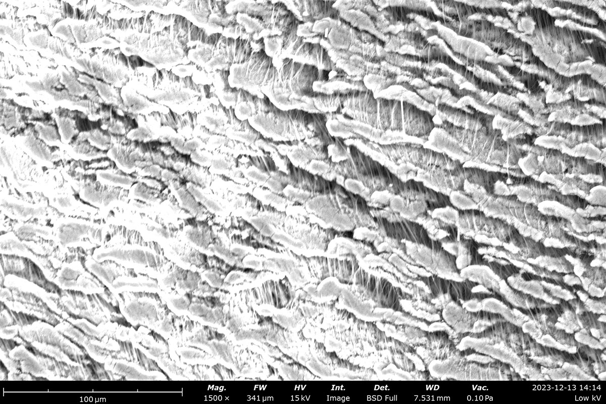
Scanning electron microscopes (SEM) function by rastering a sample with a focused beam of electrons to produce high-resolution images of the sample surface. The generated signals from these sample-beam interactions are influenced by a multitude of factors, including the energy of the electron beam. The accelerating voltage, or the potential difference between the electron source and ground measured in kilovolts, determines the kinetic energy of the beam electrons before they interact with the sample. Higher accelerating voltages are more commonly used to acquire SEM images, but the use of low accelerating voltages (low kV) has its distinct advantages. Low kV imaging can improve surface sensitivity, reduce beam-induced sample damage, and generate higher-quality images of non-conductive samples.

What Does the Accelerating Voltage Influence?
Adjusting the accelerating voltage is a critical consideration in SEM imaging as it influences the electron beam interaction volume within the sample. Once the beam electrons reach the surface of the sample, they will undergo multiple scattering events within the subsurface of the material, collectively spreading out into what is known as the interaction volume. Beam electrons with elevated kinetic energy will have a higher probability of experiencing more scattering events; each event producing a signal that is collected by the various imaging detectors within the SEM. To put it simply, the higher the accelerating voltage, the larger the interaction volume, and the greater amount of signal generation. Higher signal levels improve the signal-to-noise ratio in an image, which allows higher quality images or elemental data to be acquired faster through energy-dispersive X-ray spectroscopy (EDS). Many SEM operators tend to work at higher accelerating voltages for this exact reason.
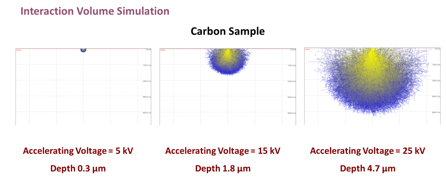
However, working at these high accelerating voltages has consequences that can obscure the results of SEM analysis. Increasing the size of the interaction volume means that more signals will be generated from within the subsurface of the sample compared to signals confined to the surface. This can be problematic when trying to analyze small or shallow features. A high-kV image may result in these shallow features becoming transparent or completely invisible due to the stronger signal from the subsurface dominating the image. The sheer amount of kinetic energy being introduced to the sample may also damage it. Delicate materials, such as organic matter and certain polymers, are extremely susceptible to being damaged by a high-energy electron beam. To avoid these outcomes, SEM operators can utilize low accelerating voltages to image their samples.
Benefits of Low-kV imaging
1. Increased surface sensitivity
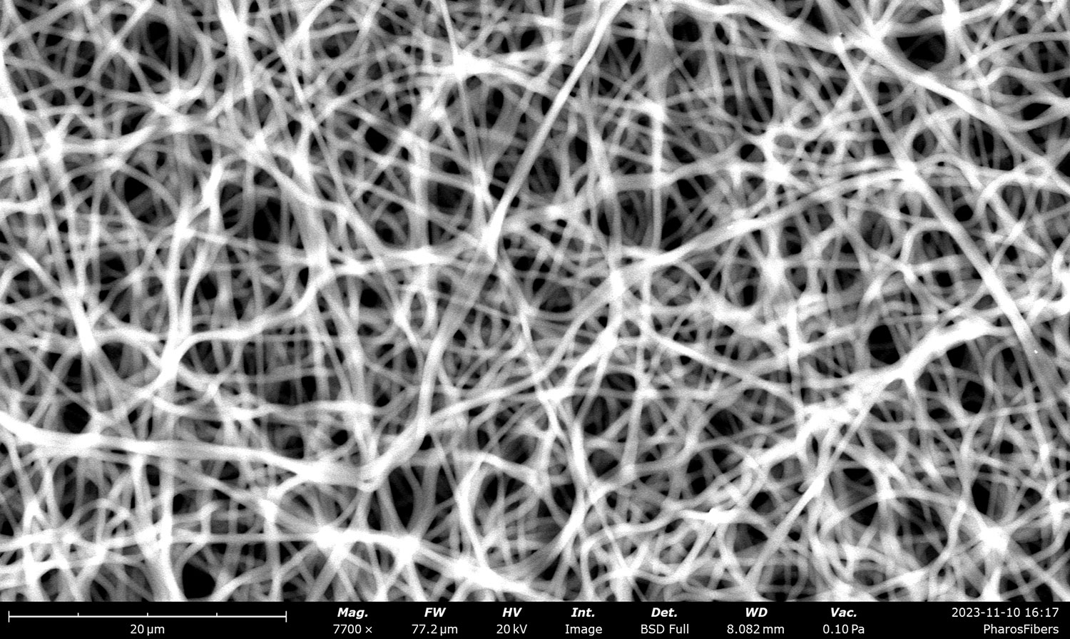
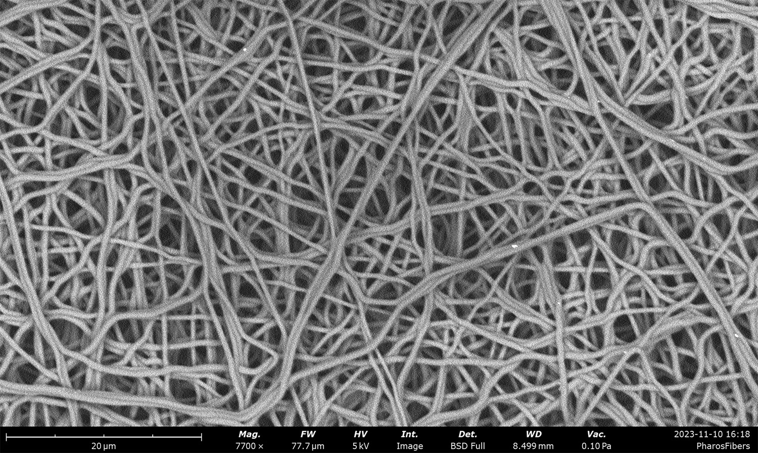
The signal generated from the sample will decrease when using a lower accelerating voltage in part because the information collected will be from a significantly smaller region. Sampling a shallower volume of interaction can increase the visibility of surface features and improve the spatial resolution of the SEM image. As an example, low kV imaging can be especially useful when looking at extremely thin samples made of carbon-rich material, such as polymer nanofibers. The SEM images below compare a nanofiber sample imaged at a high accelerating voltage (20 kV) and a low accelerating voltage (5 kV). The 20 kV image (left) demonstrates higher contrast due to the amount of signal generated, but many fibers appear transparent and in some cases are completely invisible. The 5 kV image (right) is significantly clearer as all fibers are visible and the boundaries of the individual fibers are sharply defined. The diameters of the fibers in 5 kV images match the known size while the results from the 20 kV images would underestimate the fiber diameters.
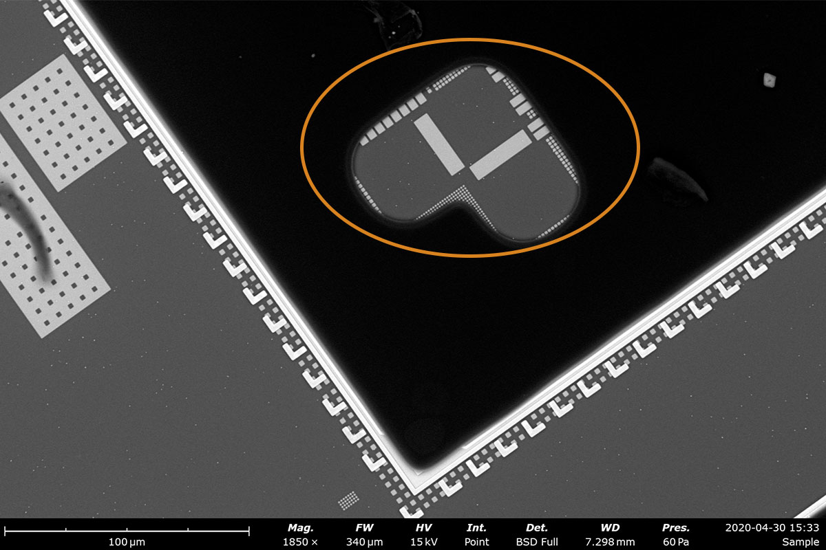
Lowering the accelerating voltage can also reveal surface features that would have been invisible otherwise. The SEM images below exhibit a semiconductor package component with a thin coating on the surface imaged at two different accelerating voltages. The thin layer on the left image (acquired at 5 kV) is no longer visible when imaged with an accelerating voltage of 15 kV because the beam electrons penetrate the subsurface metallization layers, effectively masking the surface signal. At a lower accelerating voltage, the electrons interact with the surface at a much higher ratio due to the smaller interaction volume, allowing for local analysis of the surface coating. This phenomenon is common when analyzing polymer or organic coatings on substrates such as silicon or metal. To ensure SEM images capture the surface of a thin coating or film, low kV should be used.
2. Reduced Beam Damage
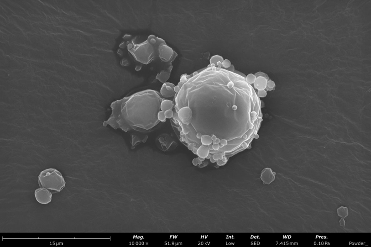
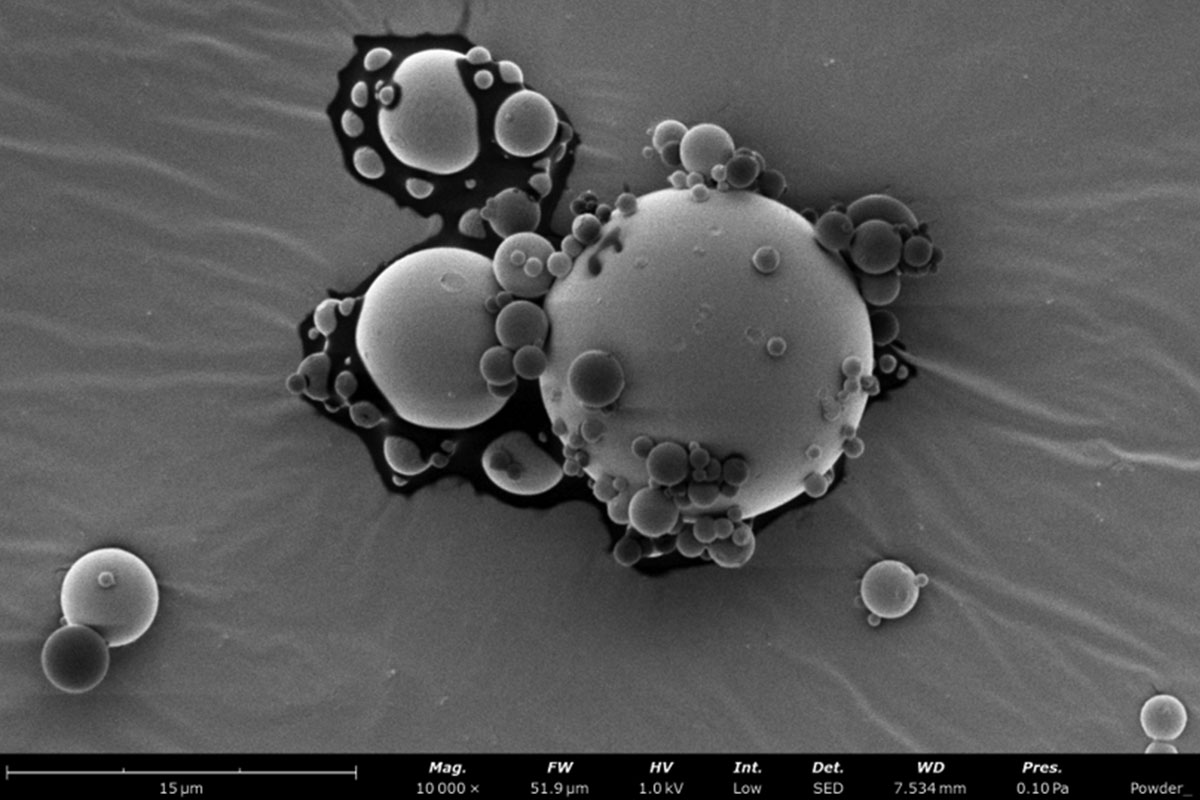
SEM analysis is considered a non-destructive analytical technique as one sample can be analyzed multiple times without permanent damage. However, delicate materials can become deformed or even destroyed with enough exposure to a high-energy electron beam. Beam damage manifests itself in several ways, from wrinkling to burning, and even to melting. Lowering the accelerating voltage when imaging these delicate samples can prevent such damage from occurring, thereby ensuring unbiased information is captured during analysis. The example below shows the difference between a pharmaceutical powder imaged at 20 kV (left) and 1 kV (right). The amount of kinetic energy being introduced to the particle at 20 kV caused it to wrinkle and shrink. The 1 kV image, however, shows a pristine, circular particle that is free of any damage. Surface texture is key in determining how a sample will behave during chemical reactions, so understanding the unaltered surface texture is vital for pharmaceutical powders.
3. Improved imaging of non-conductive samples
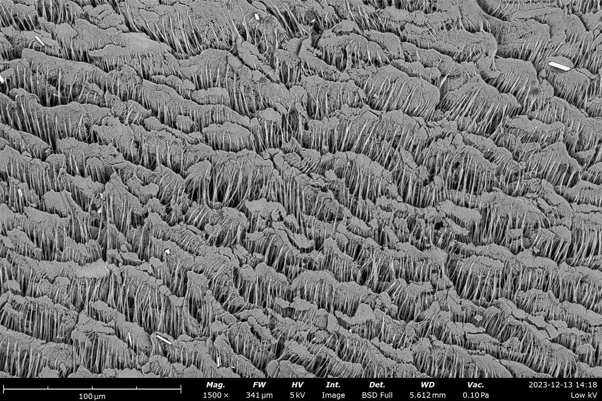
One of the most consistent challenges that SEM operators face is known as the charge effect, or the buildup of electrons on the sample surface. This occurs in non-conductive materials as they do not provide an easy escape pathway for newly introduced beam electrons. Charge buildup can severely interfere with the electron beam. The most common symptom of charging is an increase in brightness that obscures the sample from being imaged. Reducing the accelerating voltage can help mitigate charge buildup on non-conductive samples. The figure below compares PTFE tape imaged at 5 kV (left) and 15 kV (right). The 15 kV image shows overwhelming brightness that makes it difficult to discern the features of the plumber’s tape. The 5 kV image, in comparison, shows uniform brightness/contrast across the sample making features easy to observe. The structure of PTFE is responsible for the non-stick and chemical-resistant properties of this widely used sealant so knowing how to mitigate charge buildup is key for SEM analysis.
Conclusion
Lowering an SEM’s accelerating voltage can improve the imaging for several samples and applications. Even if a sample can be imaged at a higher accelerating voltage, it is good practice to start at a lower accelerating voltage to ensure a sample does not get damaged. The decreased depth the electrons travel enables sensitive samples to be imaged safely and to maximize surface feature resolution.