Batch Micro-Compounding for Lab-Scale Polymer Processing
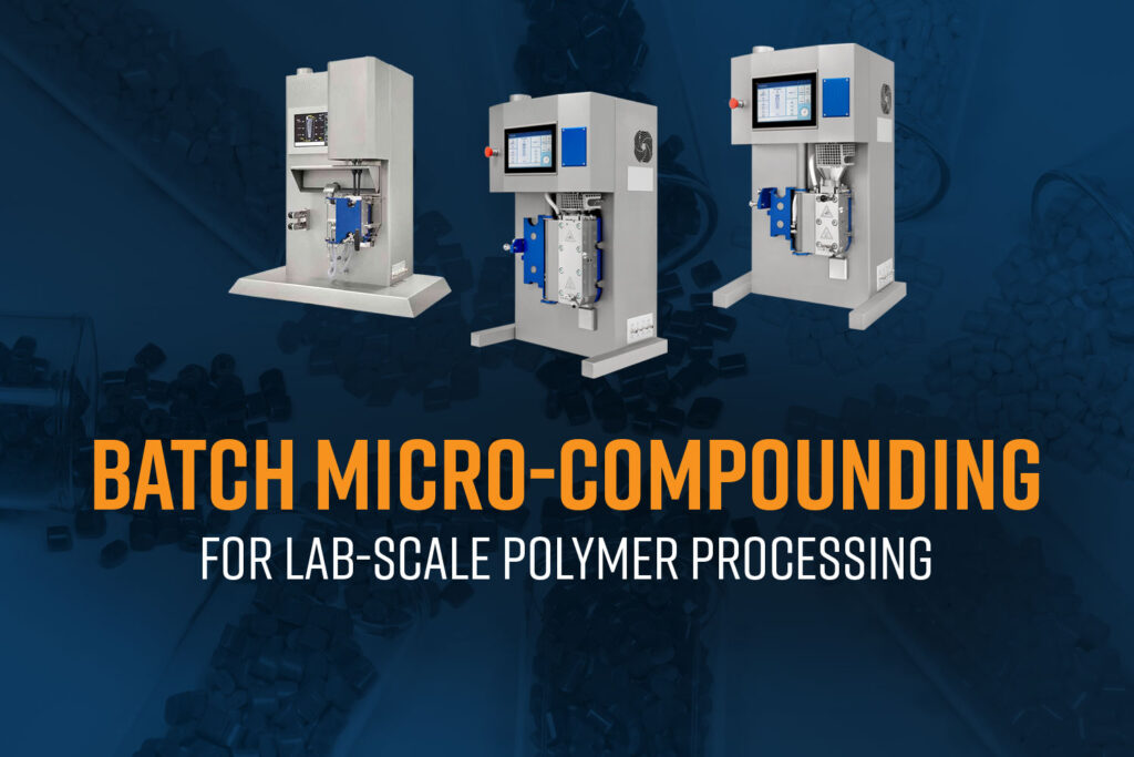
Developing new polymer materials often involves a difficult transition from concept to a testable prototype. During this early phase, researchers typically conduct multiple iterations, refining formulations, adjusting processing parameters, and evaluating material compatibility.1 Relying on large-scale production equipment for these exploratory steps can be inefficient and time-consuming. Conventional twin-screw extruders, for instance, require substantial material […]
Desktop SEM Rentals: Increasing Accessibility to Advanced Materials Analysis
Scanning Electron Microscopy (SEM) is a powerful imaging technique that enables researchers and engineers to visualize surface structures at nanometer to micrometer scales. By scanning a focused electron beam across a specimen, SEM delivers high-resolution images with exceptional depth of field, making it a critical tool for materials analysis, quality control, and failure investigation. Its ability to reveal fine morphological details, composition contrast, and microstructural features allows users to better understand how materials behave, identify defects early, and accelerate research and development.
How Much Does a QCM-D System Cost?
What is Quartz Crystal Microbalance with Dissipation Monitoring (QCM-D) and What Does it Measure? Quartz crystal microbalance with dissipation monitoring (QCM-D) instruments are powerful tools for real-time, label-free analysis of surface interactions and material properties at the molecular level. More specifically, QCM-D systems quantify nanoscale or even picoscale mass changes and viscoelastic properties in liquid-phase […]
Wettability Analysis in Semiconductor Processing
Silicon wafers are the backbone of modern electronics, forming the base material for integrated circuits, microchips, and sensors. As device features continue to shrink into the nanometer range, the cleanliness and chemical uniformity of wafer surfaces have become a critical factor in ensuring high manufacturing yields and reliable device performance. Even the smallest trace of […]
Medical Design & Manufacturing West 2026 | Feb. 3 – 5, 2026 | Anaheim, CA

MD&M West – Medical Design & Manufacturing West Nanoscience Instruments, together with our sister company, Nanoscience Analytical, provide advanced instrumentation and contract R&D services that support the design, prototyping, and scale-up of medical devices and biomedical materials. Our solutions are widely used in the medical device industry with applications in developing tissue scaffolds, vascular grafts, […]
Ten Factors that Influence the Cost of QCM-D Systems
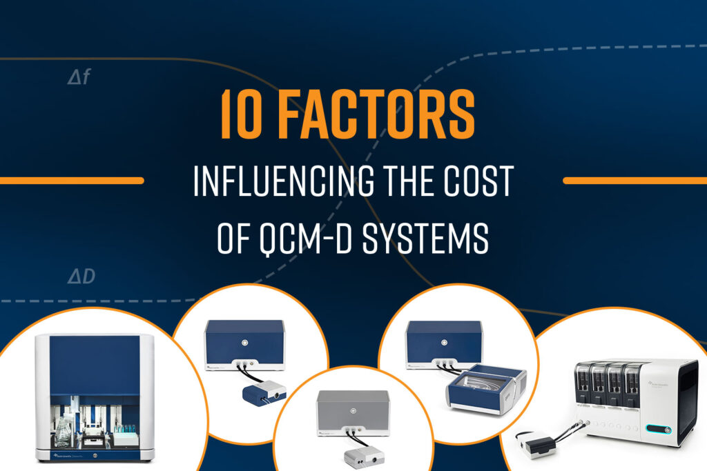
Quartz crystal microbalance with dissipation monitoring (QCM-D) instruments are powerful tools for real-time, label-free analysis of molecular interactions on a surface in a liquid environment. QCM-D systems can quantify nanoscale mass changes and viscoelastic properties of thin films on the surface in adsorption or desorption studies., If you are curious about adding QCM-D to your […]
The Hidden Costs of Polymer Compounding in R&D
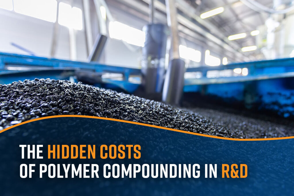
Polymer compounding is fundamental to developing new polymeric materials in sectors such as automotive, aerospace, medical devices, and packaging. While traditional compounding methods remain prevalent in research and development (R&D) environments, they often come with hidden costs that impact time and resources. What Is Traditional Polymer Compounding? Traditional polymer compounding usually operates on industrial principles […]
2-Day SEM Short Course | Alexandria, VA | April 2026

2-Day SEM Short Courses: Explore the microscopic world in our specialized 2-day Scanning Electron Microscopy (SEM) Short Course. Held in Alexandria, VA, this immersive program is designed for both experienced practitioners and newcomers, offering an in-depth exploration of both fundamental and advanced SEM techniques. Hosted at our state-of-the-art facilities, the course features hands-on sessions with […]
Broad Ion Beam vs. Focused Ion Beam Polishing: Choosing the Right Technique for Sample Preparation
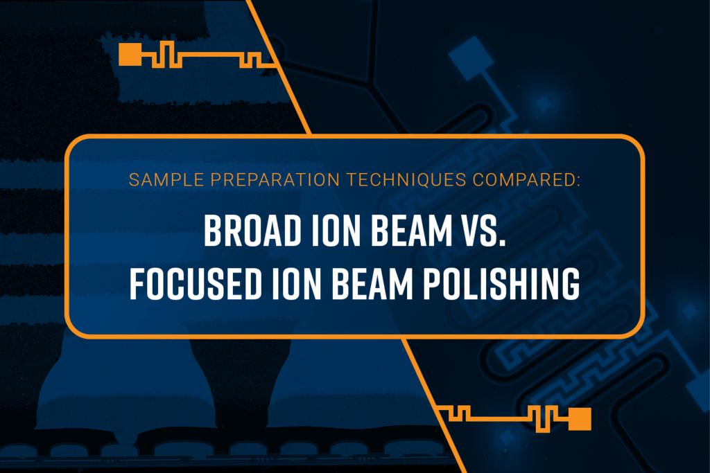
When preparing samples for electron microscopy, the choice of method directly impacts the clarity and reliability of the images. Imperfections such as roughness, contamination, or surface damage can obscure fine details and lead to misinterpreted data. Ion beam polishing, also known as ion beam milling, is an advanced sample preparation method that uses a directed […]
What is a Twin Screw Extruder? Types, Applications, and Benefits Explained

Twin screw extruders are among the most versatile processing equipment used in polymer compounding, pharmaceutical hot-melt extrusion, food production, and advanced materials research. They provide the precision and flexibility needed for complex formulations. Twin screw extruders offer superior mixing, enhanced process control, and facile scalability making them indispensable in industries where performance and consistency are […]