Microscopy & Microanalysis 2026 | Aug 3-6, 2026 | Milwaukee, WI
Join us in Salt Lake City, Utah for the highlight of the microscopy calendar – M&M 2025! Nanoscience Instruments is back for this annual summertime conference, and this time we’re showcasing in Booth #1925.
Nanoscience Instruments Expands Polymer Processing Solutions through Strategic Partnership with Fontijne Presses
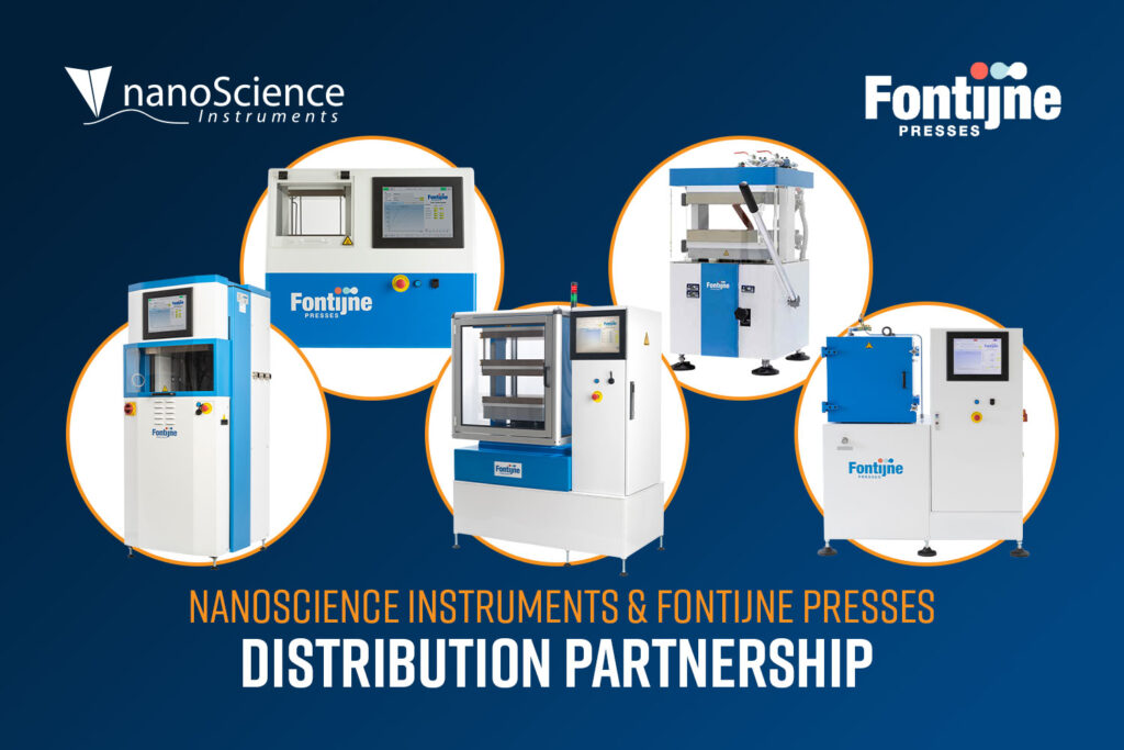
New Partnership Brings Advanced Laboratory Platen Press Solutions to North American Researchers Nanoscience Instruments is pleased to announce a new strategic partnership with Fontijne Presses, a globally recognized manufacturer of precision laboratory platen presses. Through this agreement, Nanoscience Instruments will serve as the exclusive distributor of Fontijne Presses systems in North America, expanding its portfolio […]
Phenom Pharos STEM: Bringing True STEM Capability to the Desktop
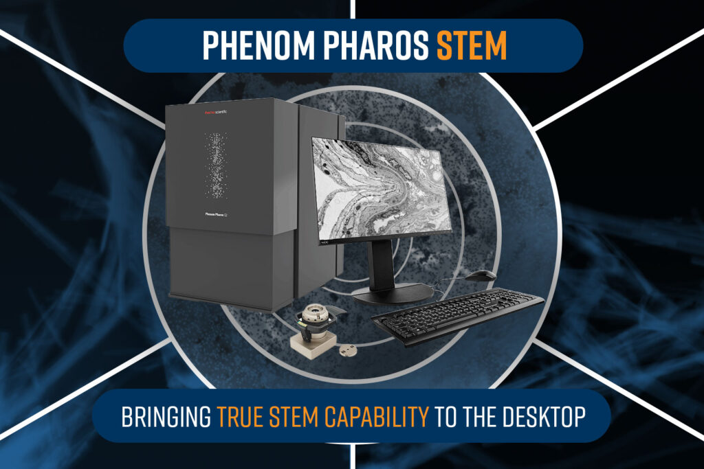
Scanning Transmission Electron Microscopy (STEM) is a scanning-based imaging technique that uses a focused electron beam to raster scan across an ultra-thin sample, typically <150 nm. Although STEM is similar to Scanning Electron Microscopy (SEM), it differs fundamentally in how electrons interact with the sample and how signals are generated (comparison shown in Table 1). […]
2-Day SEM Short Course | Phoenix, AZ | Nov. 4 – 5, 2026
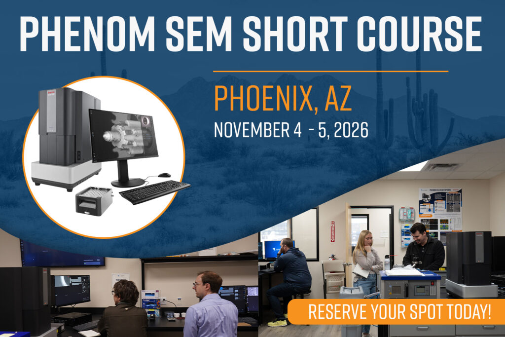
2-Day SEM Short Course: Explore the microscopic world in our specialized 2-day Scanning Electron Microscopy (SEM) Short Course. Held in Phoenix, AZ, this immersive program is designed for both experienced practitioners and newcomers, offering an in-depth exploration of both fundamental and advanced SEM techniques. Hosted at our state-of-the-art facilities, the course features hands-on sessions with […]
2-Day SEM Short Course | Alexandria, VA | Sept. 2 – 3, 2026
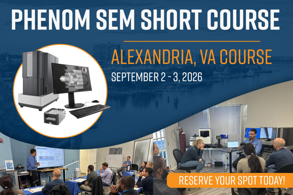
2-Day SEM Short Courses: Explore the microscopic world in our specialized 2-day Scanning Electron Microscopy (SEM) Short Course. Held in Alexandria, VA, this immersive program is designed for both experienced practitioners and newcomers, offering an in-depth exploration of both fundamental and advanced SEM techniques. Hosted at our state-of-the-art facilities, the course features hands-on sessions with […]
2026 NanoNews: SEM Edition Q1
How Wettability Analysis Improves Semiconductor Package Performance and Reliability
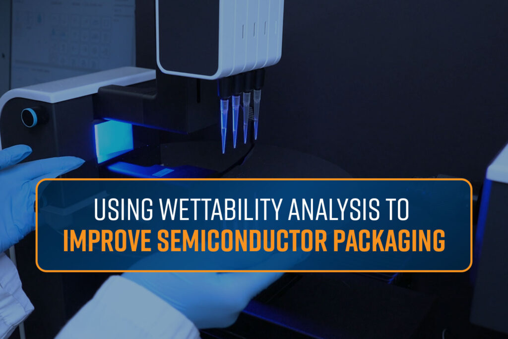
As semiconductor devices continue to shrink and packaging architectures grow more complex, surface interactions play an increasingly important role in overall performance and reliability. Wettability analysis has become a key quality and process-control tool across the semiconductor packaging workflow. From solder joint formation to underfill flow and photoresist coating behavior, understanding how liquids interact with […]
Improving Life Science EM Imaging using AI
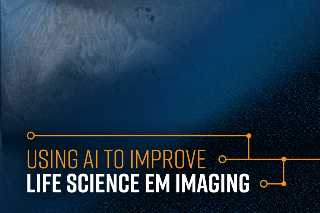
Electron Microscopy in Life Sciences There are a number of common electron microscopy methods deployed in life sciences for imaging. The basic entry-level is Scanning Electron Microscopy (SEM) used for magnifications beyond optical microscopes, up to 1 million times magnification. Next comes Transmission Electron Microscopy (TEM) which plays a critical role in life sciences by […]
Improving 4D-STEM Efficiency Through AI
Researchers use 4D-STEM to extract quantitative information about strain, electric and magnetic fields, crystal structure, defects, and local chemistry. What are the common challenges in 4D-STEM? Despite its immense capabilities, 4D-STEM comes with significant practical challenges including: Dose and Beam Damage 4D-STEM often requires high electron doses to capture clear, high-contrast 4D-STEM images. This can […]
AISTech 2026 | May 4-6, 2026 | Pittsburgh, PA
Association for Iron & Steel Technology Conference 2026 At Nanoscience Instruments, we empower steelmakers by equipping them with the means to achieve comprehensive inclusion analysis in one automated system: desktop scanning electron microscopy (SEM) combined with energy dispersive X-ray spectroscopy (EDS). Automated SEM-EDS forms the functional backbone of the Phenom ParticleX Steel system, elevating high […]