Scanning Electron Microscopy (SEM) generates high-resolution images by scanning a focused beam of electrons across the sample surface and detecting the signals produced through beam-sample interactions. Imaging nonconductive samples by SEM poses a challenge since they accumulate electrostatic charge at their surface during imaging, resulting in a variety of imaging artifacts. Therefore, mitigating the effects of charge accumulation is essential for ensuring reliable SEM analysis of non-conducting materials.
While sputter coating a thin metal layer is a common approach for mitigating charging in nonconductive samples, many types of samples and analyses may not be compatible with this technique. As an alternative, variable pressure mode or low vacuum mode can be used to effectively reduce charging effects when imaging uncoated samples in the SEM. This blog explains the benefits of variable pressure imaging in SEM and provides several examples to showcase the analysis of different types of non-conductive materials.

What Are the Downsides of Charging?
Nonconductive samples can exhibit charging effects when imaged under high vacuum conditions. Charging occurs when electrons accumulate on the surface of an insulating material, leading to imaging artifacts. These artifacts can include distortions, blurring, and alterations in contrast, ultimately impacting the accuracy and clarity of the SEM images obtained.Even minor charging can result in inaccurate dimensional measurements and affect the interpretation of SEM results by obscuring critical microstructural details. Figure 1 illustrates the two most common downsides of charging when SEM imaging: a loss of contrast and image distortions.

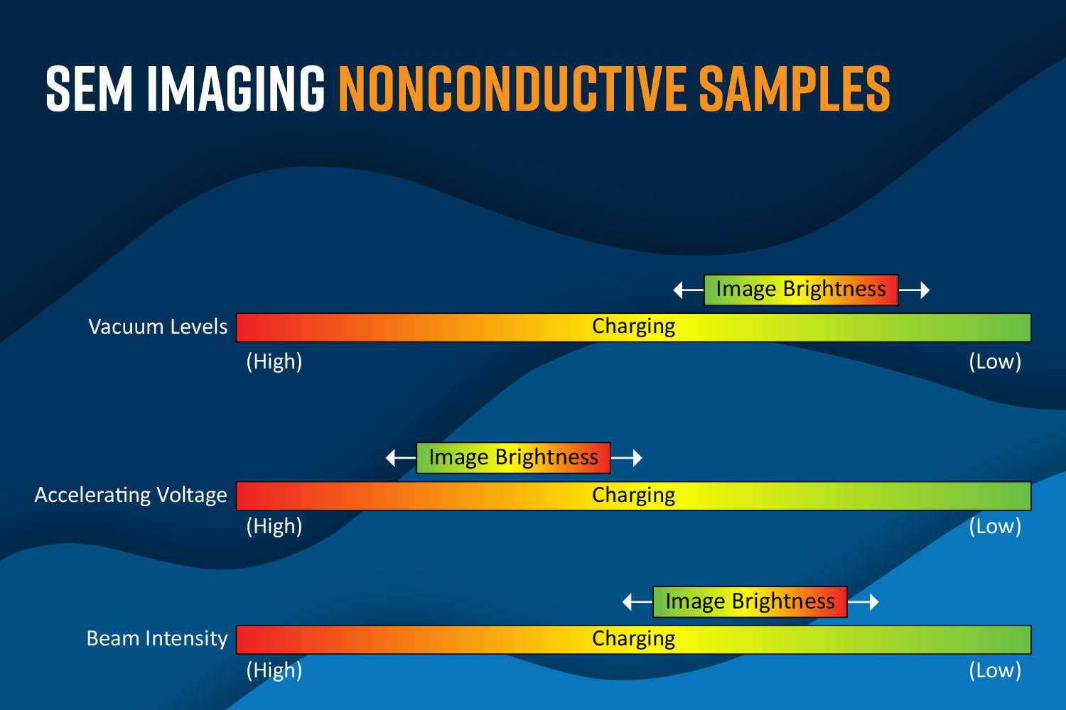
How Does the Chamber Pressure Affect Charging?
The vacuum level within the SEM sample chamber plays a critical role in charging and thereby in the quality of the images obtained. For most (conductive) samples, a higher vacuum is preferred due to its ability to produce higher-brightness images with less noise. However, imaging non-conductive samples in high vacuum levels results in charge accumulation on the sample surface. Lowering the vacuum level in the SEM chamber can help mitigate charging effects by increasing the number of gas molecules present. These gas molecules provide a pathway for electrons to dissipate, reducing the buildup of charge on the sample surface.
Using Variable Pressures to Optimize the Imaging of Non-conductive Samples
In the examples shown in Figure 2, several non-conductive samples are imaged under high and low vacuum conditions. Under conventional high vacuum conditions, the images demonstrate some degree of contrast alterations and blurring making it difficult to visualize the topographical features on the sample. Under low vacuum conditions, the artifacts introduced due to charging have been minimized resulting in notably crispier images across the entire field of view and are free of skewed contrast.
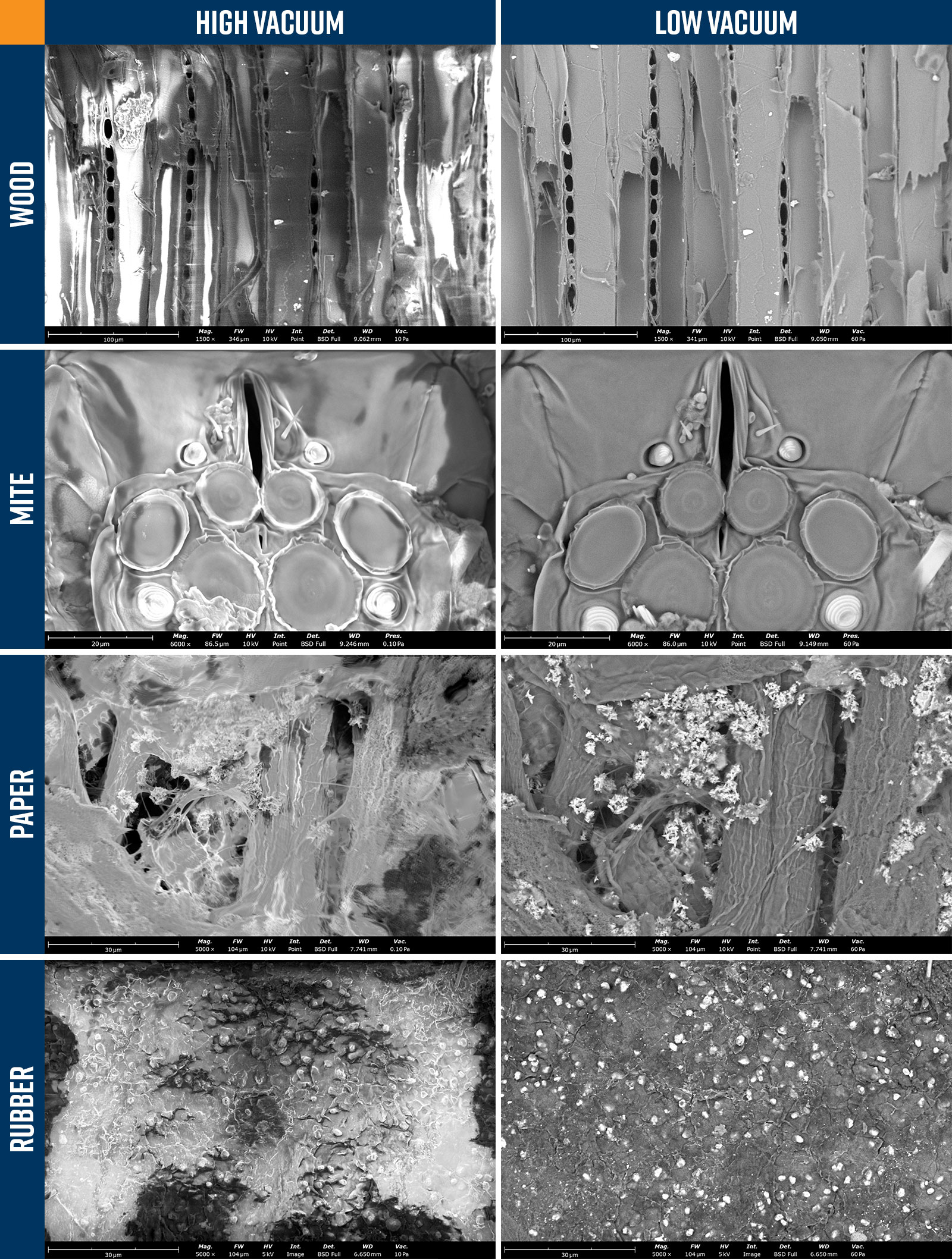
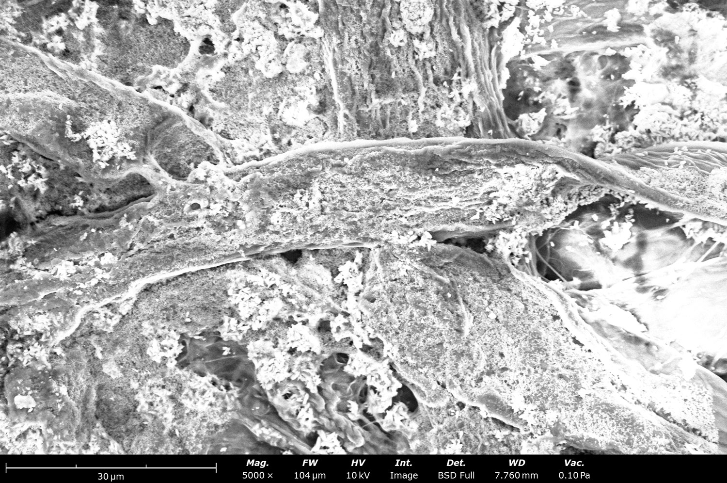
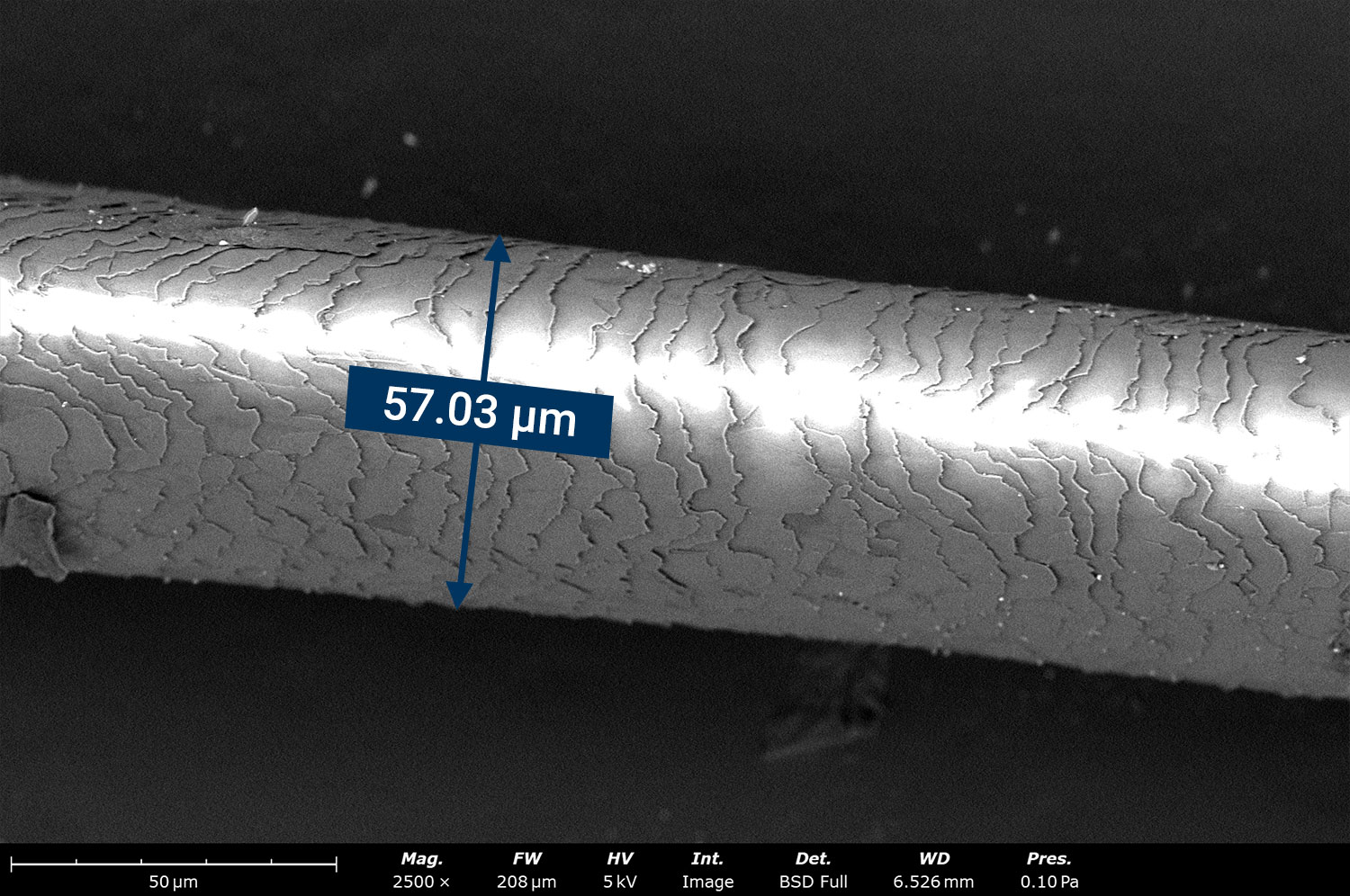
Charging not only decreases the quality of an image but can also alter the size or orientation of features within an image. In the example of the images of mites from Figure 2, the central vertical cavity bends to the left when the sample is charging but when imaged in low vacuum, the cavity appears straighter and slightly longer. These slight distortions can be detrimental, especially when measurements are taken from the image. For example, the topological features of the hair in Figure 3 can be seen even when the image is charging, but the measured diameter varies significantly compared to when the hair is at low vacuum and not charging.

Optimizing Beam Parameters
Although lowering the vacuum can reduce charging, the electron beam parameters sometimes need to be adjusted as well to produce the optimal image. In low vacuum mode, the increased number of gas molecules within the chamber will interact with the beam electrons and increase noise levels resulting in deterioration of the image quality.
To combat this, beam parameters need to be adjusted such that the signal generated from the sample is enhanced. Increasing the accelerating voltage effectively speeds up the electrons, which increases their depth of penetration. This increases the number of electron-sample interactions and effectively increases the signal-to-noise ratio. Increasing the beam intensity can also produce a similar effect.
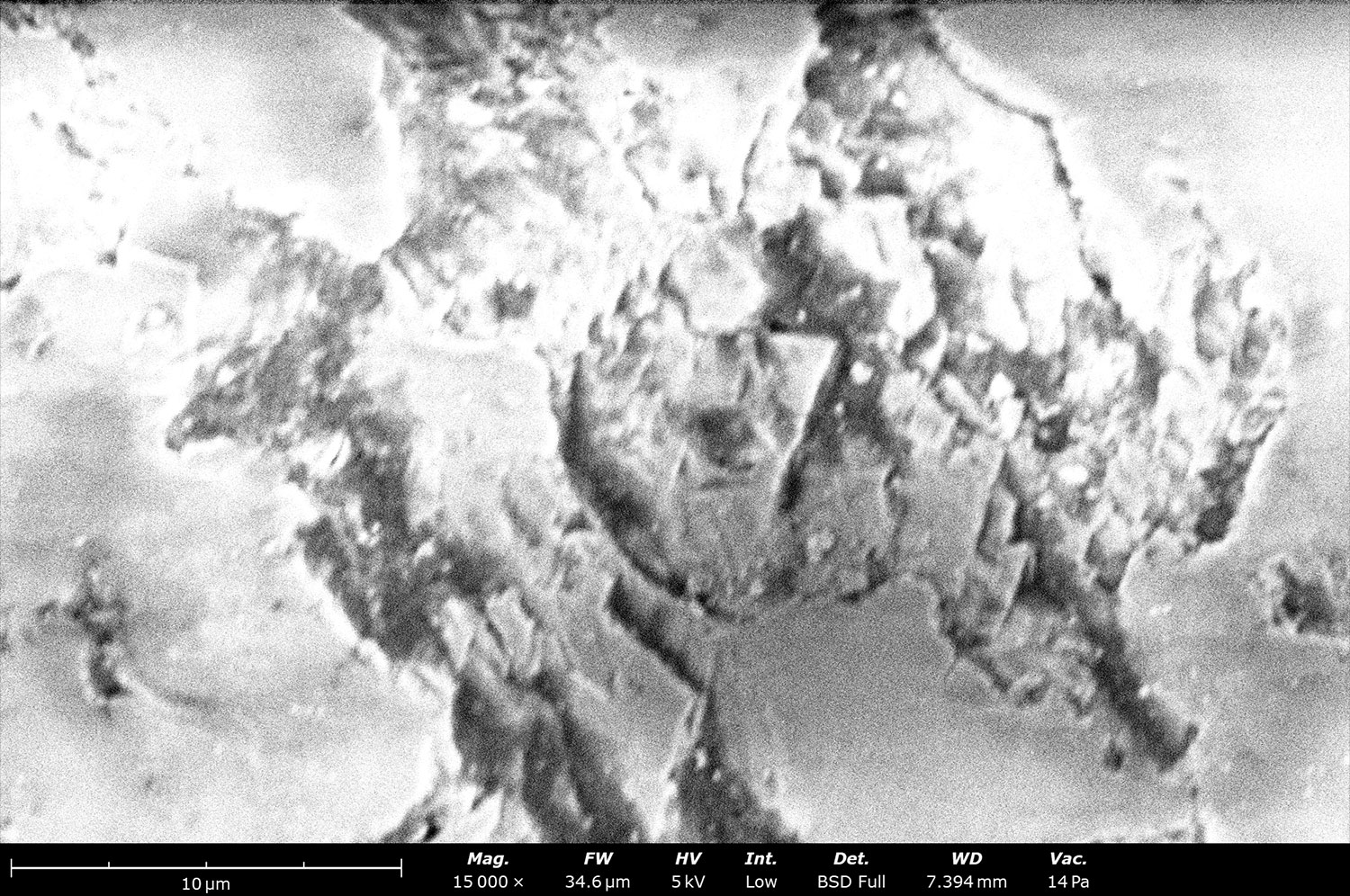
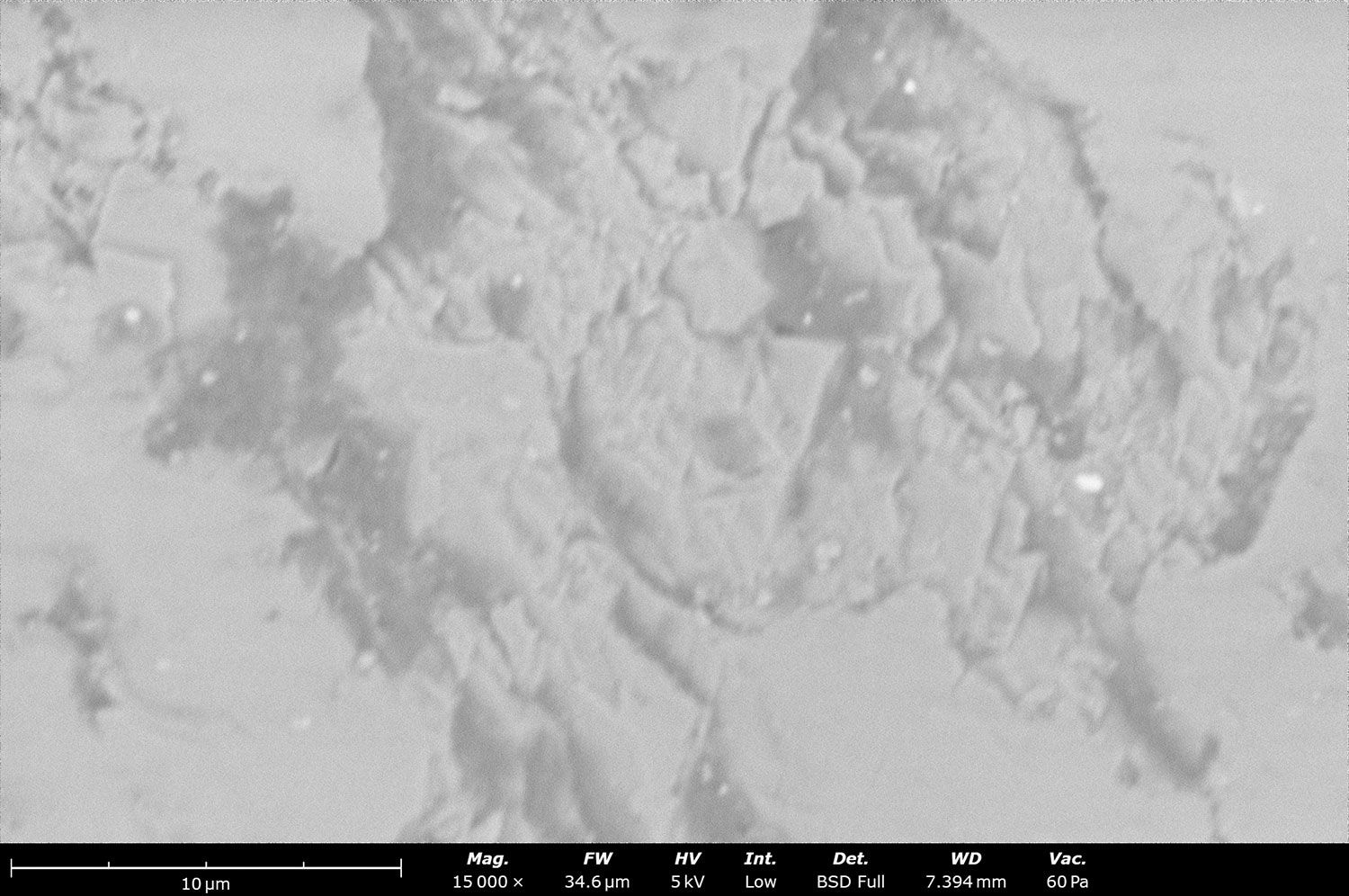
For example, a nonconductive piece of rock imaged using an SEM shows severe charging artifacts even at a pressure of 10 Pa while using a low beam intensity (Figure 4). When the chamber pressure is increased to 60 Pa, the contrast distortions seen previously are minimized but the image produced shows dramatically reduced contrast due to the added noise resulting from the additional gas molecules. When both the accelerating voltage and intensity are increased, the signal-to-noise ratio improves, and a sharper image is produced that is free of charging artifacts.

Summary
Imaging artifacts frequently occur when using SEM to image non-conductive samples due to the charging effect of the samples. The charging effects can be minimized by employing variable pressure imaging, which involves increasing the number of gas molecules thereby reducing the vacuum levels in the chamber. The increase in the number of gas molecules allows electrons built up on the surface to dissipate. Fine-tuning the beam parameters in conjunction with adjusting the chamber pressure can significantly enhance image quality. This technique is especially valuable for imaging non-conductive samples in scenarios where sputter coating is not feasible.