As semiconductor devices continue to shrink and packaging architectures grow more complex, surface interactions play an increasingly important role in overall performance and reliability. Wettability analysis has become a key quality and process-control tool across the semiconductor packaging workflow. From solder joint formation to underfill flow and photoresist coating behavior, understanding how liquids interact with device surfaces directly affects yield, reliability, and long-term device stability. In this article, we explore where wettability analysis fits into modern semiconductor packaging and why it has become essential for advanced manufacturing.

What Is Wettability and Why Does It Matter?
Wettability describes how a liquid interacts with and spreads across a solid surface. At a fundamental level, it reflects the balance between adhesive forces (between the liquid and the surface) and cohesive forces (within the liquid itself). When adhesive forces dominate, the liquid spreads easily across the surface; when cohesive forces dominate, the liquid forms droplets with minimal spreading.
In semiconductor manufacturing, many packaging processes depend on liquids, such as solders, adhesives, encapsulants, and photoresists, spreading in a controlled and predictable manner across device surfaces. Liquids must spread predictably during processes such as underfill dispensing or photoresist coating. Poor wetting can lead to voids, incomplete coverage, or uneven films. Adhesives and encapsulants require good wetting to form strong interfacial bonds. Insufficient wetting can lead to delamination or mechanical failure. Solder joints depend on proper wetting between molten solder and metal pads. Poor wetting can produce weak joints or electrical discontinuities.
Several factors can influence wettability on semiconductor surfaces. These include contamination introduced during handling or processing, oxide formation on metal surfaces, residual solvents or cleaning agents, surface treatments such as plasma activation or chemical priming, and variations in surface roughness. Even small changes in these conditions can significantly alter wetting behavior. Hence, wettability analysis is often used as a rapid diagnostic tool for surface preparation and process validation.
Contact angle measurement for wettability analysis
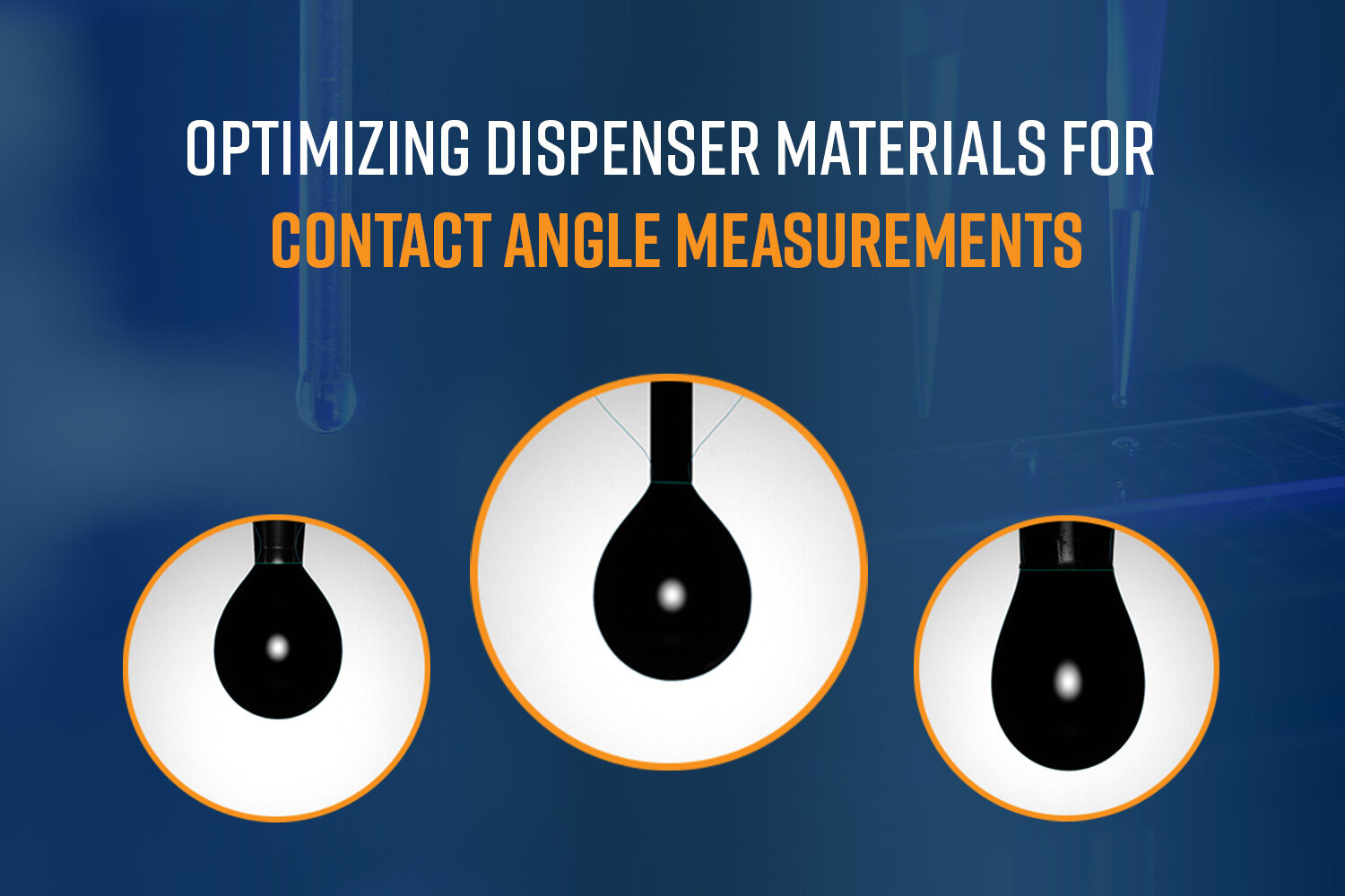
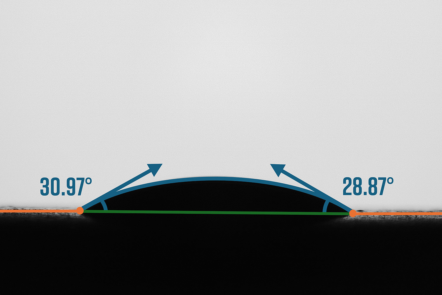
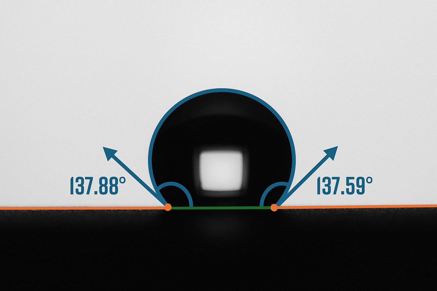
One of the most used methods to measure the degree of wettability is contact angle measurements.1 The contact angle is the angle formed at the interface where the liquid, solid, and vapor phases meet. This measurement provides a simple but powerful indicator of how the surface will behave in real manufacturing environments. If the contact angle is low (< 90°), it indicates good wetting, where the liquid spreads across the surface. High contact angles (> 90°) indicate poor wetting, where the liquid beads up. Complete or near-complete wetting is inferred if the contact angle is very low (< 10°). A visualization of this can be seen in Figure 1.
Because many semiconductor packaging processes rely on controlled spreading of liquids, such as solder fluxes, adhesives, photoresists, and encapsulants, contact angle measurements provide valuable predictive insight into process performance.
Key Applications of Wettability Analysis in Semiconductor Packaging
Solderability and Interconnect Quality:
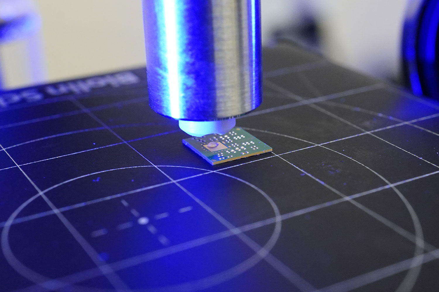
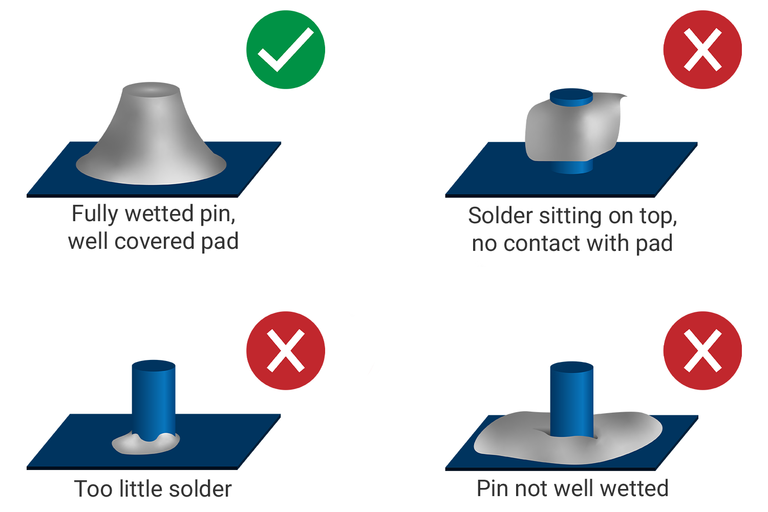
Reliable solder joints are fundamental to semiconductor package performance. During assembly processes such as flip-chip bonding, ball grid array (BGA) formation, and wafer-level packaging, molten solder must spread uniformly across metallized pads to create strong electrical and mechanical connections.2 Poor wetting can result in several reliability issues, including, non-wetting or partial wetting of solder pads, voids or incomplete solder joints, irregular solder ball formation and increased electrical resistance in interconnects as shown in Figure 2.
Wettability analysis helps engineers evaluate how well solder or solder flux interacts with surfaces such as copper, nickel, gold, or protective finishes. Contact angle measurements provide insight into whether the surface energy of the pad supports proper solder spreading.
Underfill and Encapsulation Flow Optimization:
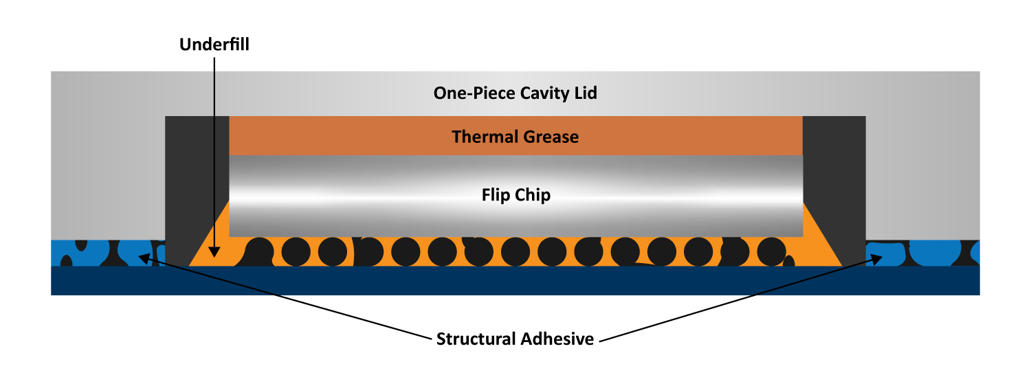
Flip-chip packaging requires the use of underfill materials to enhance mechanical stability and protect solder joints from thermal and mechanical stress. Underfill materials are dispensed along the edge of the die and must flow by capillary action into narrow gaps between the die and substrate (Figure 3). Wettability plays a critical role in determining how effectively the underfill material spreads within these small spaces. If wetting is insufficient, the underfill may not fully penetrate the gap, resulting in trapped air pockets or voids.
Wettability analysis helps optimize surface energy balance between the silicon die and substrate, compatibility between the underfill formulation and packaging materials and surface preparation methods such as plasma cleaning. Ensuring proper wetting improves capillary flow, reduces void formation, and enhances the long-term mechanical reliability of the package.
Adhesion Performance in Die-Attach Processes:
Die-attach materials such as epoxies, silver-filled adhesives, or sintering pastes are widely used to secure semiconductor dies to substrates or lead frames. Strong adhesion at the interface is essential for mechanical stability and efficient thermal conduction. Surface conditions that can affect adhesion include organic contamination from processing steps, oxidation of metal surfaces, incomplete surface cleaning and inconsistent plasma or chemical treatments.
Good adhesion typically requires that the adhesive material adequately wets the bonding surfaces. Wettability measurements help engineers determine whether the surface energy of the substrate supports proper spreading and bonding of the adhesive. By monitoring contact angles before bonding, manufacturers can confirm that surfaces are properly prepared to support strong adhesive interfaces.
Uniform Photoresist and Coating Deposition:
Many semiconductor fabrication and packaging steps involve applying thin liquid films, such as photoresists, dielectric coatings, or protective polymers. These films must spread evenly across wafer or substrate surfaces to produce uniform thickness and defect-free coverage. Wettability analysis is commonly used to evaluate surface preparation prior to coating processes.3 If the surface energy is too low, the coating material may bead up or form irregular films. Conversely, proper wetting ensures smooth film formation during spin coating or dispensing.
Surface Cleanliness and Contamination Monitoring:
Surface contamination is one of the most common causes of packaging defects. Organic residues, particles, or chemical byproducts from earlier process steps can significantly alter the surface energy of semiconductor materials. Because wettability is highly sensitive to surface chemistry, contact angle measurements provide a fast method for monitoring surface cleanliness. Even trace levels of contamination can change wetting behavior and can therefore be detected through changes in measured contact angles.
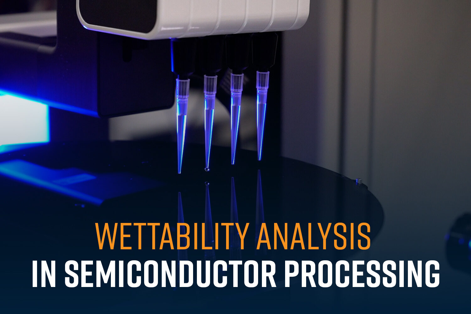
Optical Tensiometery
Optical tensiometry is a widely used analytical technique that evaluates the shape of liquid droplets on a surface using high-resolution imaging for characterizing liquid–solid interactions. By measuring properties such as contact angle and surface tension, optical tensiometers provide valuable insight into wettability, adhesion behavior, and surface energy, parameters that directly affect packaging quality and reliability.
Optical tensiometry is a non-destructive measurement technique that is highly sensitive to changes in surface chemistry. It requires minimal sample preparation and is compatible with a wide range of liquids and surfaces. These features make optical tensiometry an ideal tool for rapid analysis in process monitoring and quality control.
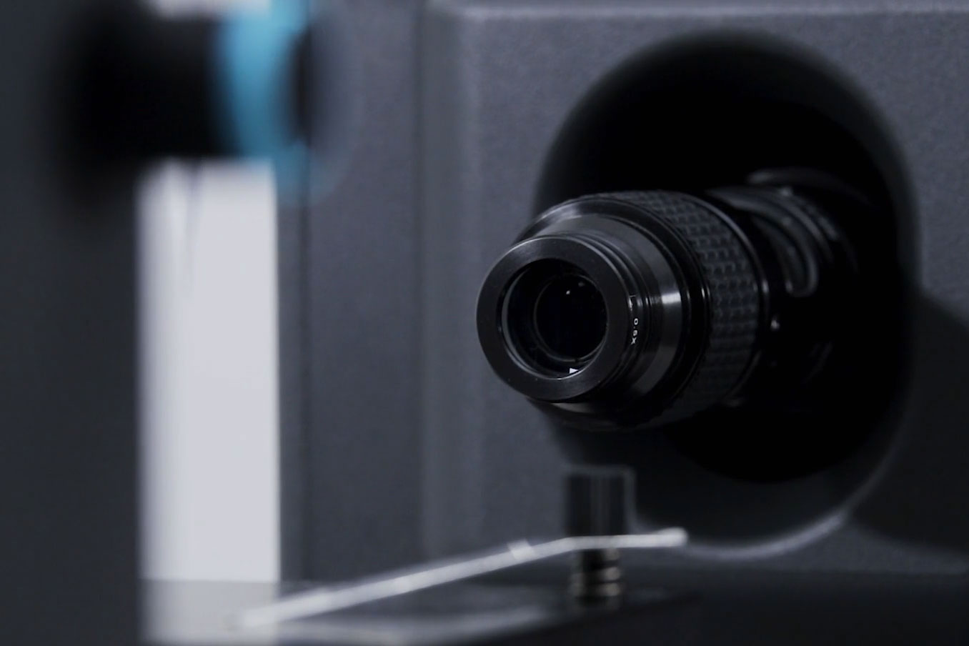
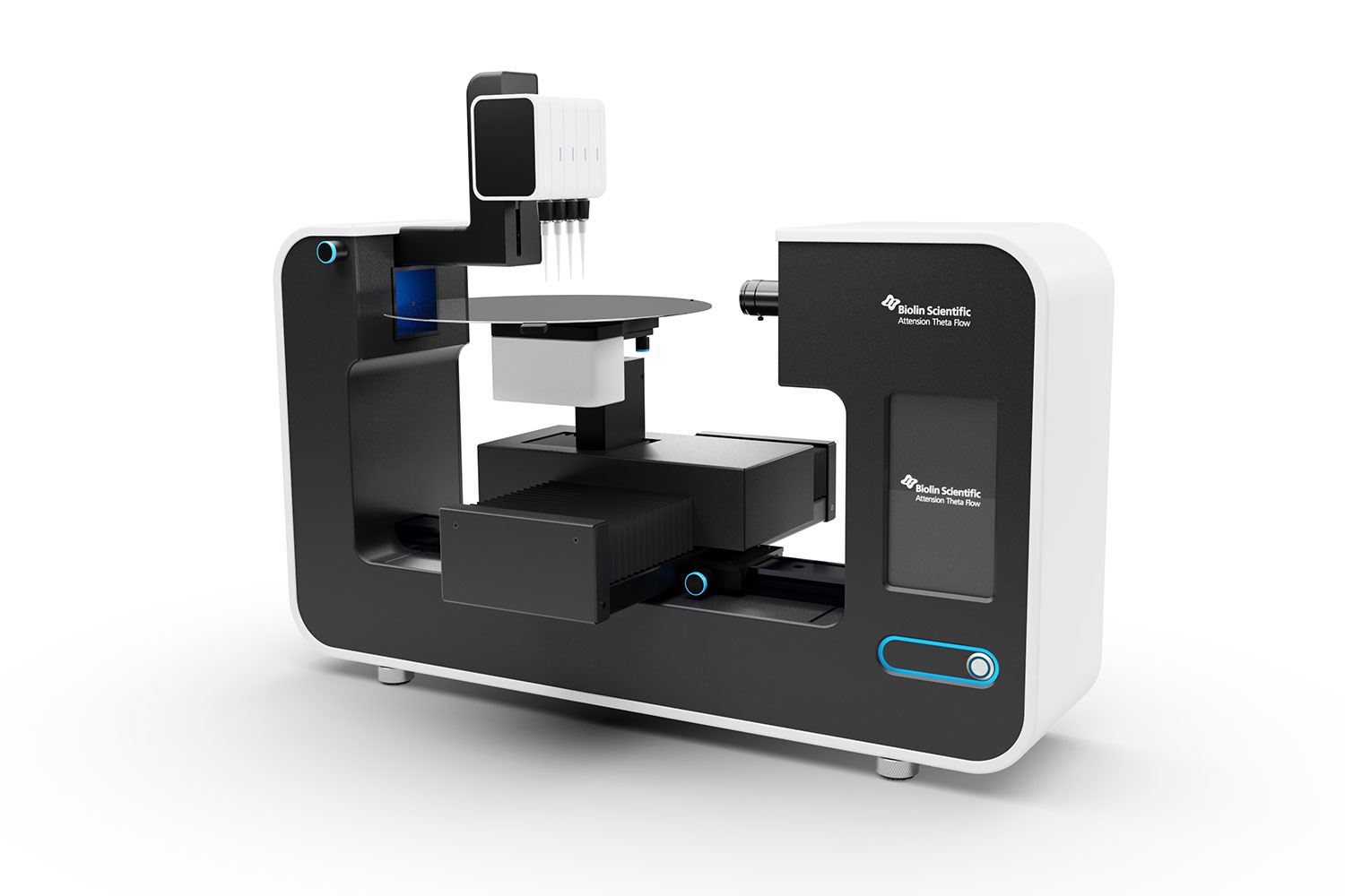
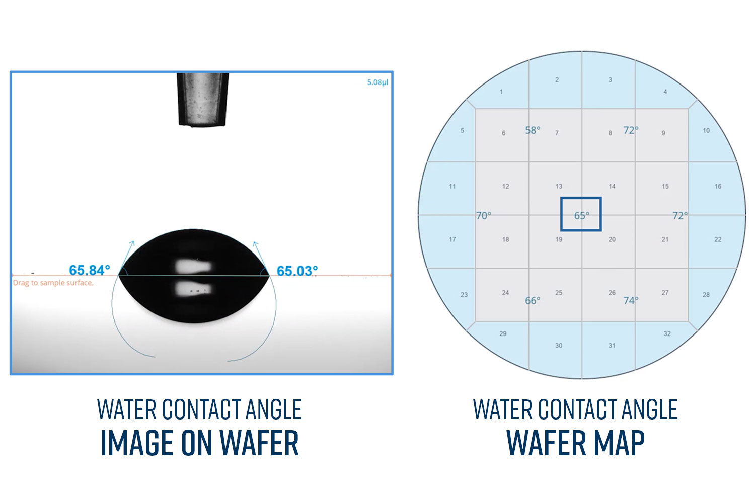
The Attension Theta Optical Tensiometer from Biolin Scientific (Figure 4A) is a versatile instrument designed for precise characterization of surface and interfacial phenomena. Using high-resolution optical imaging, the system measures contact angle, surface tension, and surface free energy to evaluate wettability and liquid–solid interactions. The Theta platform offers automated droplet dispensing, advanced image analysis, and modular configurations that support a wide range of measurement techniques, including static and dynamic contact angle analysis (Figure 4B). Its high measurement accuracy, flexible upgrade options, and user-friendly software make it particularly well suited for industrial environments where reliable surface characterization is critical for process optimization and quality control.
Conclusion
Wettability analysis has become an essential component of semiconductor packaging, supporting everything from solder joint reliability to underfill flow and coating uniformity. By understanding and controlling liquid–surface interactions, manufacturers can improve yields, reduce defects, and ensure long-term device performance. As the industry pushes toward higher density and greater functional integration, precise surface characterization tools like wettability measurement will continue to play a critical role in enabling next-generation semiconductor packaging.
References
- Kung, C. H.; Sow, P. K.; Zahiri, B.; Mérida, W. Assessment and interpretation of surface wettability based on sessile droplet contact angle measurement: challenges and opportunities. Advanced Materials Interfaces 2019, 6 (18). https://doi.org/10.1002/admi.201900839. ↩︎
- Noor, E. E. M.; Nasir, N. F. M.; Idris, S. R. A. A review: lead free solder and its wettability properties. Soldering and Surface Mount Technology 2016, 28 (3), 125–132. https://doi.org/10.1108/ssmt-08-2015-0022. ↩︎
- Dou, Y.; Li, F.; Tang, B.; Zhou, G. Surface wettability tuning of acrylic resin photoresist and its aging performance. Sensors 2021, 21 (14), 4866. https://doi.org/10.3390/s21144866. ↩︎