What is 4D-STEM?
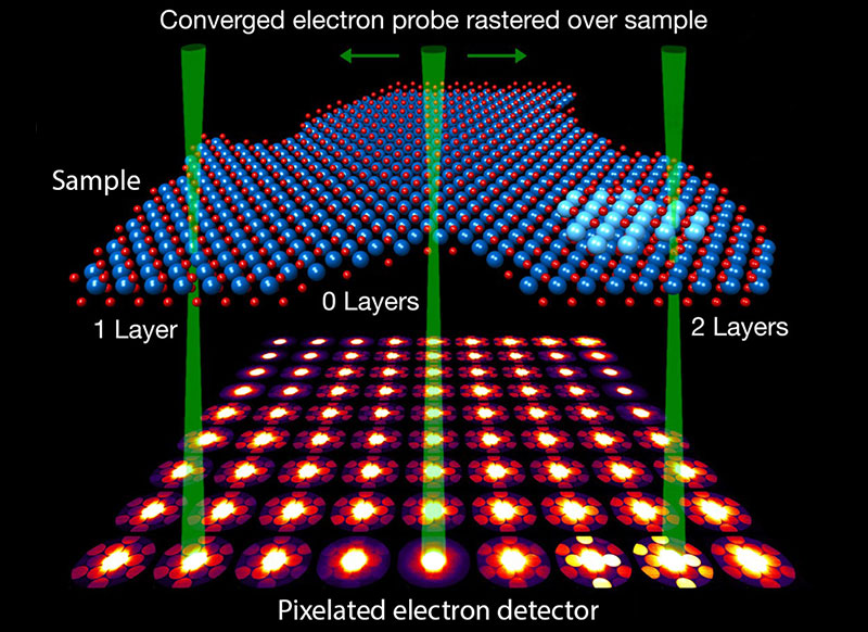
4D-Scanning Transmission Electron Microscopy (4D-STEM) is an advanced imaging technique in which a convergent beam electron diffraction pattern (CBED) is collected at each pixel, as a focused electron beam is scanned in 2D over the sample (Figure 1). This produces a rich, multidimensional dataset with two spatial dimensions and two reciprocal-space dimensions. 4D-STEM enables the use of several imaging and analytical methods from this one dataset, such as phase mapping, crystal orientation mapping, ptychography, and center-of-mass (COM) imaging, among others.1,2
Researchers use 4D-STEM to extract quantitative information about strain, electric and magnetic fields, crystal structure, defects, and local chemistry.

What are the common challenges in 4D-STEM?
Despite its immense capabilities, 4D-STEM comes with significant practical challenges including:
Dose and Beam Damage
4D-STEM often requires high electron doses to capture clear, high-contrast 4D-STEM images. This can damage beam-sensitive samples, including biological specimens, polymers, catalysts, and cryogenic materials, causing structural changes, devitrification, or even total sample loss. Managing dose is a critical part of experimental design.
Acquisition Time:
Collecting full-resolution 4D-STEM images or videos can take minutes to several hours. Long acquisition times limit throughput, increase drift and artifacts, reduce efficiency, and make it difficult to study dynamic processes. They also increase cumulative dose, further stressing sensitive samples.
Data Volume:
A single 4D-STEM dataset can reach terabytes in size. This creates significant barriers in storage, processing, data transfer, and long-term data management. In some cases, the data burden is so large that desired experiments become impractical or impossible.
What is SenseAI’s 4D-STEM Solution?
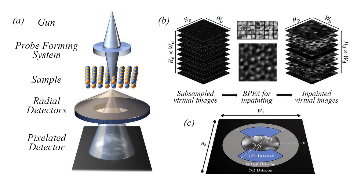
SenseAI has developed a form of compressed sensing that combines subsampling and blind dictionary-learning inpainting to greatly minimize the number of electrons and photons needed to create a full-resolution image. Instead of acquiring a complete dataset, SenseAI intentionally collects only a small subset of pixels or probe positions, sometimes as little as 1-10% of the data, and reconstructs the full image using an ultra-fast implementation of the Beta Process Factor Analysis (BPFA) algorithm, illustrated in Figure 2. For a more in-depth explanation of the BPFA algorithm, watch this recent webinar with Dr. Nigel Browning.
How does SenseAI benefit 4D-STEM users?
The key benefits of using SenseAI are three-fold: it minimizes beam damage on delicate samples; it allows faster image acquisition; and it uses up to 100x less data to capture and store those images.
By addressing the core practical constraints of 4D-STEM, SenseAI makes workflows that were once slow, destructive, or data-limited into fast, efficient, and sample-friendly processes.
Crucially, the reconstructions produced by SenseAI are mathematically validated. The algorithms cannot ‘hallucinate’ (i.e. generate new/false information, common in many forms of AI) and therefore it can only generate an image of what the object is. In some cases, the image is superior to the fully sampled ‘normal’ image due to reduced charging effects, beam damage, and even blurring.
Case Study:
Several research institutes across the globe have implemented SenseAI on their electron microscopes and are seeing significant improvements in data acquisition and analysis workflows. Here we elaborate on one such user group, the Italian National Research Council’s Institute for Microelectronics and Microsystems (CNR-IMM).
CNR-IMM, one of Europe’s leading semiconductor research labs, works with some of the largest semiconductor factories in Europe, using STEM and low-energy SEM to research the structural characterization of materials, support electron crystallography, and carry out customized imaging. They also perform cryogenic TEM measurements on radiation sensitive materials such as graphene or polymers.
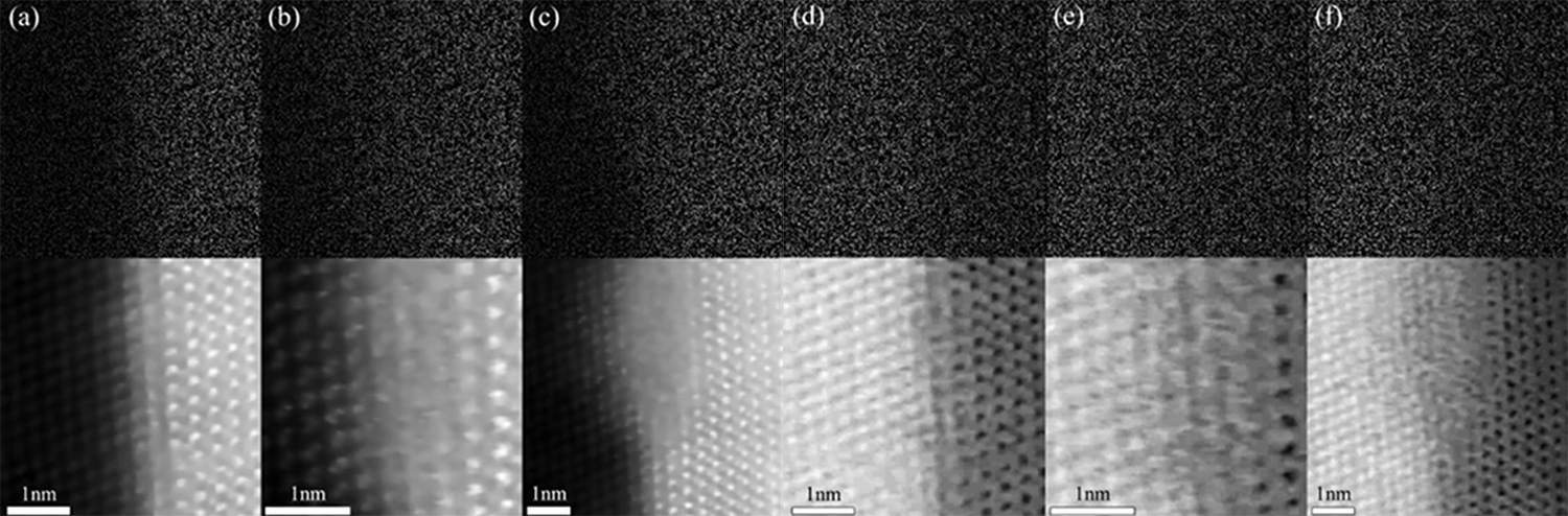
CNR-IMM has started using SenseAI to achieve faster alignment with a lower electron dose. They rapidly test different parameters to get the maximum output from their analysis. This approach is illustrated by the data in Figure 3. Giuseppe Nicotra, Head of Sub-Ångstrom Electron Microscope LAB at CNR-IMM says: “In the semiconductor industry many specimens are very beam-sensitive. With SenseAI we can work at previously unachievably low doses to preserve sample integrity and benefit from superior data.”
Thanks to SenseAI’s ability to perform analysis across SEM, TEM, and 2D and 4D-STEM in real-time, users can tune settings in the moment to improve their images, saving significant amounts of time throughout each imaging session. Dr. Nicotra explains, “There’s nothing worse than when you acquire a 4D-STEM data set and you’re unable to know how good it is until you’ve processed and analysed it. If the results are not satisfactory, then must re-acquire the datasets. This is a lengthy process consuming huge amounts of data. With SenseAI you can see 4D-STEM images live and adjust on the fly.”
Finally, Dr. Nicotra speaks to the benefits of a responsive, real-time solution: “For electron microscope operators, it’s important to have a very reactive system, especially when you are tuning imaging parameters – you need very fast feedback. Tuning imaging parameters with SenseAI was great, and I’m really impressed at how SenseAI denoises, refines, and reconstructs very noisy images.”
The group at CNR-IMM also explored compressive sensing for faster, more efficient electron energy loss spectroscopy (EELS), which is particularly useful for their applications due to its sensitivity to low-mass elements and ability to determine oxidation states, chemical bonding, and spatial distribution. They successfully demonstrated that SenseAI’s technology can use just 25% of the original data and achieve functionally identical results to the full-resolution, fully sampled dataset.5 This work opens the door to faster, lower-dose STEM-EELS for potentially beam sensitive or beam-reactive dynamic materials.
Conclusion
SenseAI’s technology represents a major step forward in electron microscopy, offering a practical solution to one of the field’s most persistent challenges, balancing efficiency, image quality, and data volume. By integrating advanced subsampling algorithms with real-time image reconstruction, SenseAI empowers researchers in 4D-STEM to capture high-quality data faster and more efficiently, while preserving the integrity of even the most delicate samples.
References
- Zuo, J.-M.; Zhu, X. Strategies for fast and reliable 4D-STEM orientation and phase mapping of nanomaterials and devices. Microscopy and Microanalysis 2021, 27 (S1), 762–763. https://doi.org/10.1017/s1431927621003044. ↩︎
- Li, G.; Zhang, H.; Han, Y. 4D-STEM Ptychography for Electron-Beam-Sensitive Materials. ACS Central Science 2022, 8 (12), 1579–1588. https://doi.org/10.1021/acscentsci.2c01137. ↩︎
- Ophus, C. Four-Dimensional scanning Transmission Electron Microscopy (4D-STEM): from scanning nanodiffraction to ptychography and beyond. Microscopy and Microanalysis 2019, 25 (3), 563–582. https://doi.org/10.1017/s1431927619000497. ↩︎
- Robinson, A. W.; Moshtaghpour, A.; Wells, J.; Nicholls, D.; Chi, M.; MacLaren, I.; Kirkland, A., I.; Browning, N. D. Simultaneous High-Speed and Low-Dose 4-D STEM using compressive sensing techniques. arXiv (Cornell University) 2023. https://doi.org/10.48550/arxiv.2309.14055. ↩︎
- Robinson, A.; Wells, J.; Nicholls, D.; Nicotra, G.; Browning, N. Fast and low dose EELS using compressive sensing. BIO Web of Conferences 2024, 129, 06020. https://doi.org/10.1051/bioconf/202412906020. ↩︎