Silicon wafers are the backbone of modern electronics, forming the base material for integrated circuits, microchips, and sensors. As device features continue to shrink into the nanometer range, the cleanliness and chemical uniformity of wafer surfaces have become a critical factor in ensuring high manufacturing yields and reliable device performance. Even the smallest trace of organic residue, metallic contamination, or particulate matter can alter electrical properties and compromise production.
To prevent product and time waste in further steps, it is critical to validate critical moments during wafer processing. Many of these steps, such as initial cleaning or photoresist adhesion, are impacted by the chemical properties of the surface. One of the most effective and widely adopted tools for assessing wafer surface quality is contact angle measurement.1 This straightforward technique provides valuable insights into wafer cleanliness, making it an indispensable quality control method in semiconductor manufacturing.
In this blog, we will discuss how wettability analysis with optical tensiometry is a fundamental tool for characterizing surface chemistry, particularly after cleaning steps and during semiconductor processing with photoresist adhesion.

Contact Angle Measurement: A Window into Surface Chemistry
Contact angle measurement is based on observing how a droplet of liquid interacts with the wafer surface. Contact angle measurements can be easily made with an optical tensiometer (also known as a goniometer). An optical tensiometer uses a high-resolution camera and advanced software to quantify the intermolecular interactions between a liquid droplet and solid surface. For this measurement, a liquid droplet is placed onto a solid surface with an automatic dispenser, while a high-performance camera captures images of the droplet profile. The droplet profile is fitted automatically with a software algorithm, giving the angle at the edges of the droplet tangent to the surface. This angle is directly proportional to the chemical interactions between the liquid, solid and vapor phases at this interface at the monolayer level. Using a probe liquid like water, we can determine surface cleanliness or verify important chemical alterations of the surface. If we want to assess the efficacy of liquid-based coatings, we can also determine the level of adhesion, as indicated with smaller contact angles.
Low contact angle indicates high wettability, which is characteristic of clean or hydrophilic surfaces. High contact angle suggests the presence of contaminants or hydrophobic layers. This simple principle allows engineers to quickly determine whether a wafer is sufficiently clean for downstream processing. The main advantages of this technique are that it is fast, accurate, repeatable, non-destructive, quantitative and cost effective.
Contact Angle Analysis for Surface Cleanliness
Every silicon wafer undergoes numerous processing steps such as slicing, chemical-mechanical polishing (CMP), thermal oxidation, deposition and etching. The performance and reliability of semiconductor devices depend heavily on the cleanliness of the silicon wafer substrates during and after each step in the process. Even microscopic contamination, organic residues, metal ions, or airborne particulates, can introduce defects during subsequent processing steps. These defects may lead to poor thin-film adhesion, reduced lithography accuracy, electrical leakage, or device failure. Maintaining pristine wafer surfaces is therefore essential to ensure manufacturing yield and device longevity.
To maintain wafer cleanliness, industry-standard cleaning protocols are used to remove both organic and inorganic impurities. Validating the success of these cleaning steps requires sensitive, reliable evaluation techniques. Contact angle measurement is an effective way to monitor surface cleanliness and provides valuable insights into the state of the wafer surface and cleaning process, making it an indispensable quality control method in semiconductor manufacturing.
Contact Angle Analysis of HMDS Treatment for Photoresist Adhesion
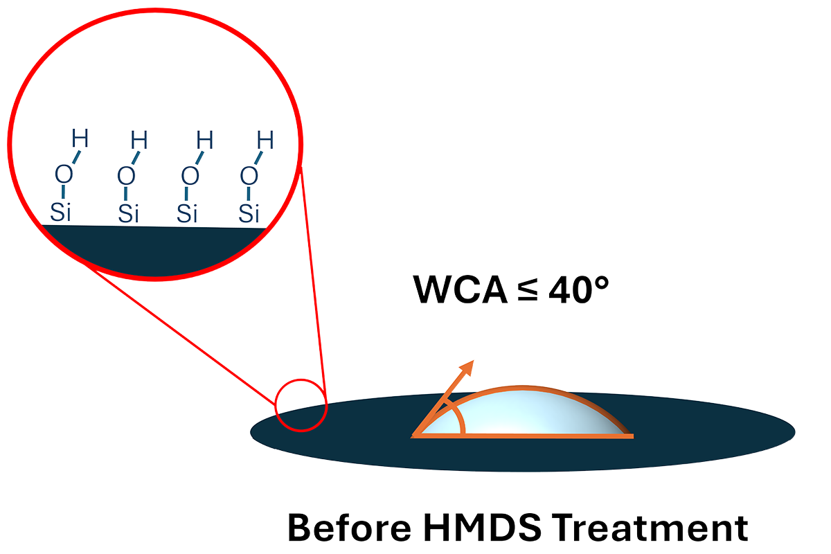
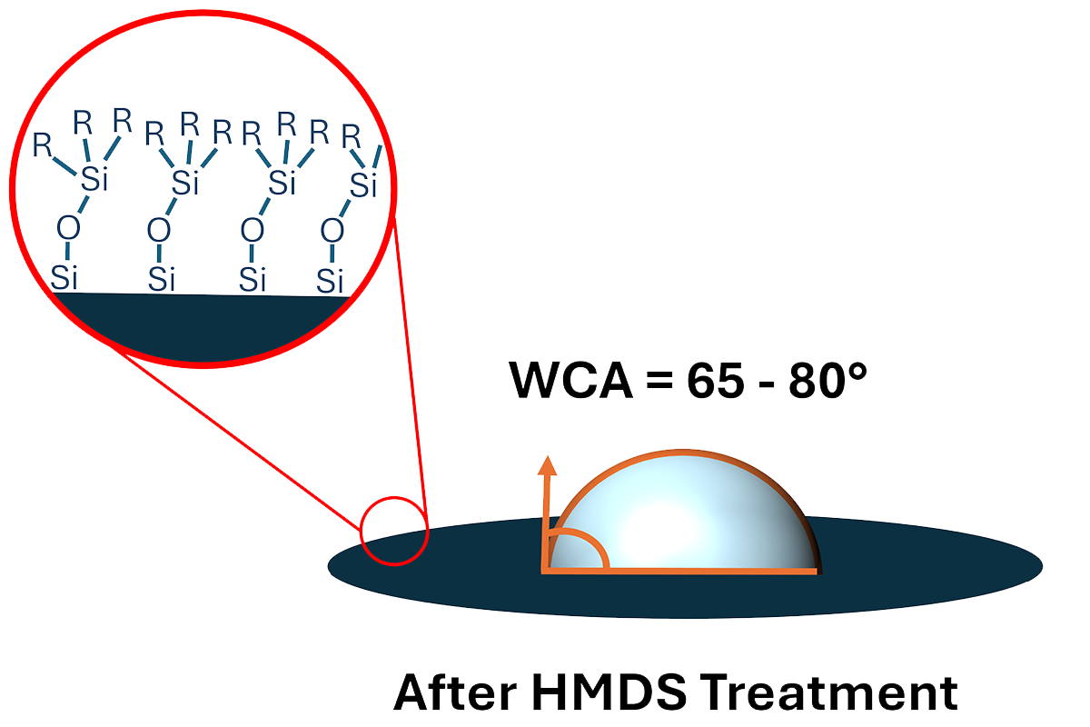
During wafer processing, many of the layered patterns are created using photolithography and a photoresist coating. Having adequate photoresist adhesion to the wafer surface is paramount for successful lithographic steps, with delamination of the photo resist resulting in patterning errors that can be detrimental to the devices’ execution. After the initial wafer cleaning, the wafer surface is terminated with hydroxide chemical groups, rendering the surface hydrophilic. Cleanliness can be determined with a low water contact angle, but this is not ideal for good adhesion with the polymer-based binder present in the photoresist formulation. To improve the adhesion, typically the Si wafer is treated with hexamethyldisilazane (HMDS). This process was originally patented by R.H. Collins and F.T. Deverse of IBM in 1970.2 While this method has evolved over the years from solution to vapor-based methods, HMDS is used to chemically silanize the previously hydroxyl terminated Si wafer, resulting in a hydrophobic surface that better matches the molecular properties of the photoresist. Prior to the HMDS treatment, the water contact angle on the bare Si surface is at or below 40°, illustrated in Figure 1a. If the HMDS priming step is successful, the water contact angle increases significantly, usually in the 65-80° range, which is demonstrated in Figure 1b.
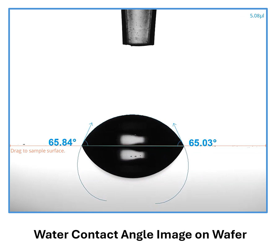
For this process, a coupon or dummy wafer can be sent along with the wafer batch and tested before and after the HMDS treatment. With the test wafer, multiple points of the wafer surface should be mapped out to ensure full coating coverage, such as the experiment shown in Figure 2, which measured water contact angle in 7 different locations across the wafer. A lack of increase in water contact angle from before and after HMDS treatment or a large variation in the water contact angle may indicate failure or unevenness in the wafer priming process.

Conclusion
Optimizing photoresist adhesion is a critical procedure in wafer processing in the semiconductor and electronics industries. An important step is treating the wafer with HMDS to have high quality photoresist adhesion. Water contact angle measurements with an optical tensiometer are a powerful method to quickly and easily validate the quality of this process. With automated wafer mapping, this can be verified on multiple points of a wafer to ensure completeness of coating.
References:
- Kung, C. H.; Sow, P. K.; Zahiri, B.; Mérida, W. Assessment and interpretation of surface wettability based on sessile droplet contact angle measurement: challenges and opportunities. Advanced Materials Interfaces 2019, 6 (18). https://doi.org/10.1002/admi.201900839. ↩︎
- Robert H Collins, R. H.; Deverse, F. T. Process for improving photoresist adhesion. U.S. Patent 354936A, December 22, 1970. ↩︎