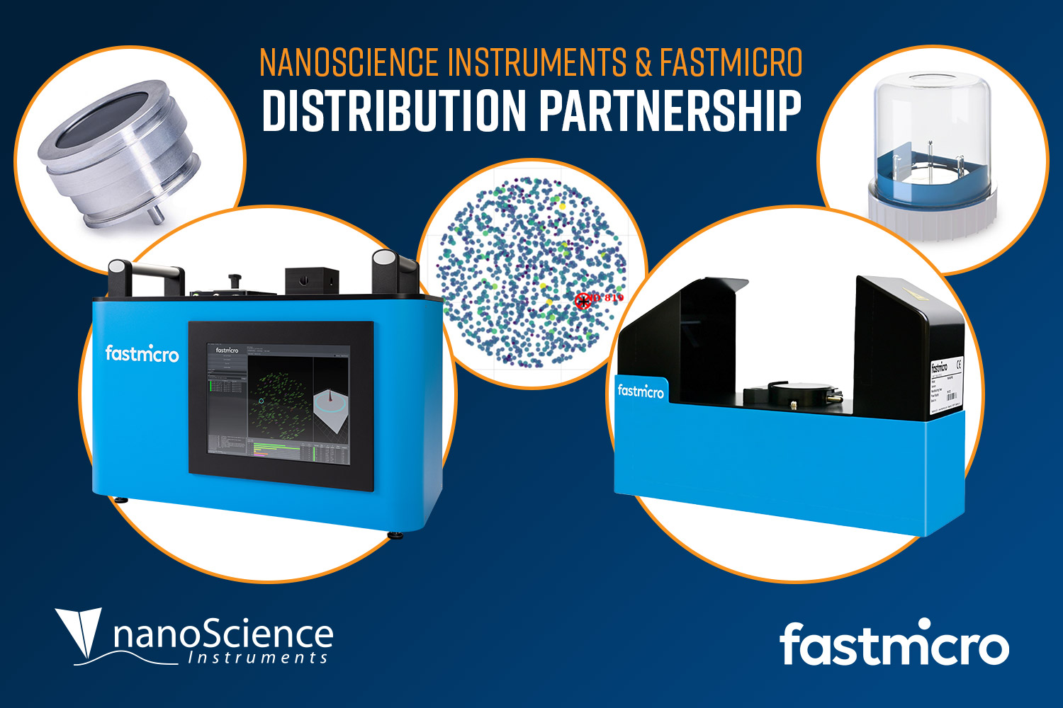
Combined technologies enable faster and more effective surface particle contamination analysis Phoenix, AZ — Nanoscience Instruments is pleased to announce a strategic partnership with Fastmicro,…
Posted: June 30, 2026

Join us in Salt Lake City, Utah for the highlight of the microscopy calendar – M&M 2025! Nanoscience Instruments is back for this annual summertime…
Posted: June 24, 2026

New Partnership Brings Advanced Laboratory Platen Press Solutions to North American Researchers Nanoscience Instruments is pleased to announce a new strategic partnership with Fontijne Presses,…
Posted: June 2, 2026
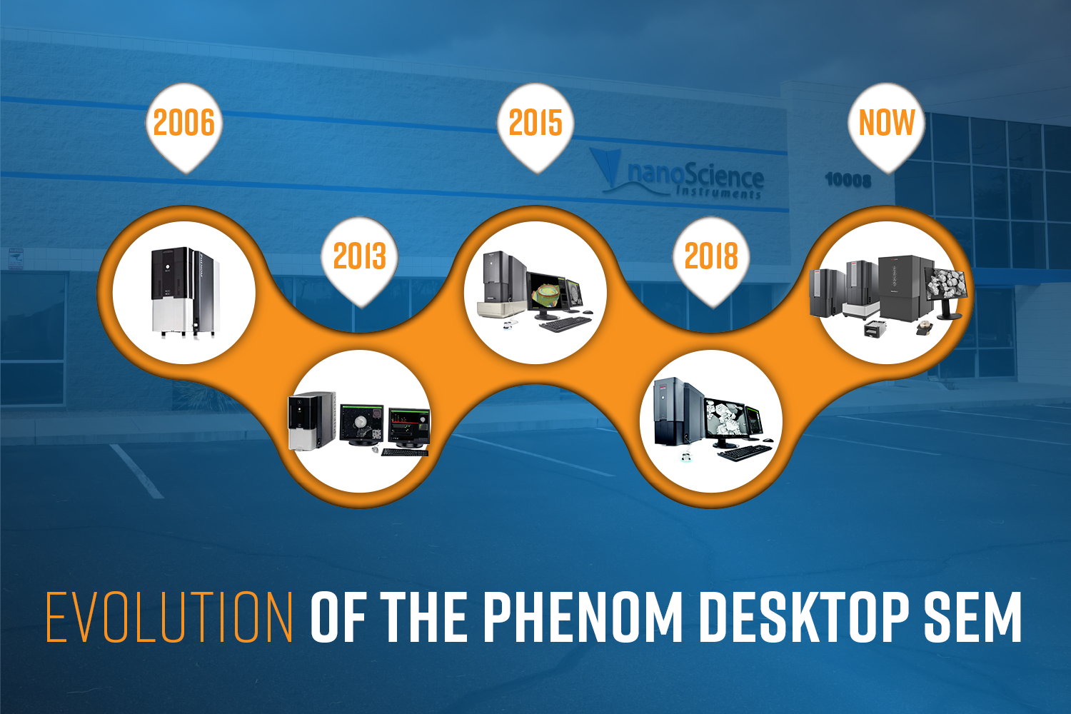
The Phenom Scanning Electron Microscope (SEM) is turning 20 this year! In celebration of this milestone, it is worth reflecting on how the platform has…
Posted: May 13, 2026
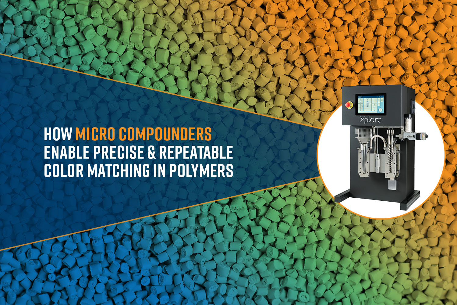
Color matching in polymer compounding involves formulating and adjusting pigments, dyes, and additives to achieve a precise, repeatable target color, an essential requirement for ensuring product…
Posted: May 6, 2026
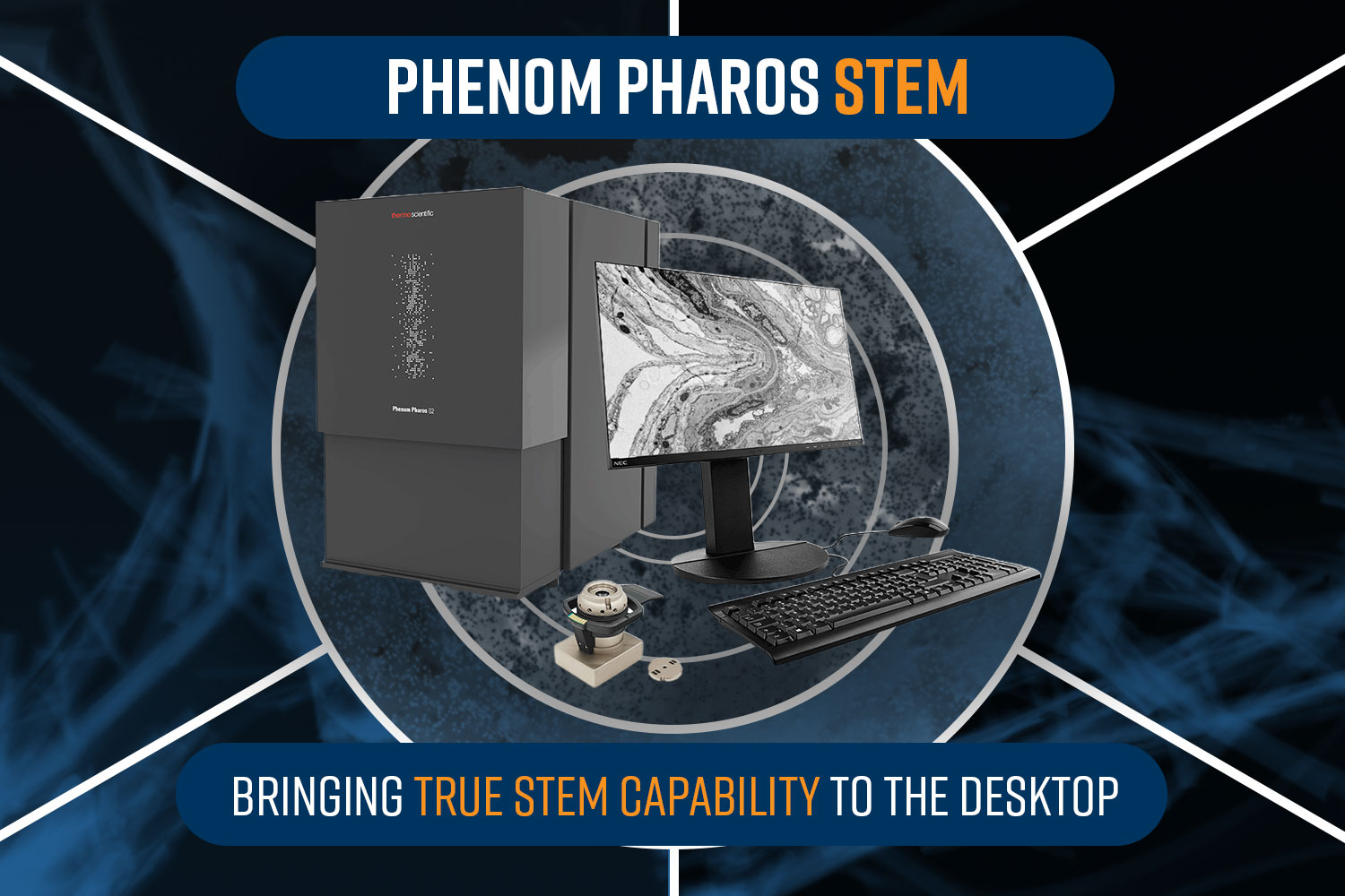
Scanning Transmission Electron Microscopy (STEM) is a scanning-based imaging technique that uses a focused electron beam to raster scan across an ultra-thin sample, typically <150…
Posted: April 29, 2026

2-Day SEM Short Course: Explore the microscopic world in our specialized 2-day Scanning Electron Microscopy (SEM) Short Course. Held in Phoenix, AZ, this immersive program…
Posted: April 9, 2026

2-Day SEM Short Courses: Explore the microscopic world in our specialized 2-day Scanning Electron Microscopy (SEM) Short Course. Held in Alexandria, VA, this immersive program…
Posted: April 9, 2026
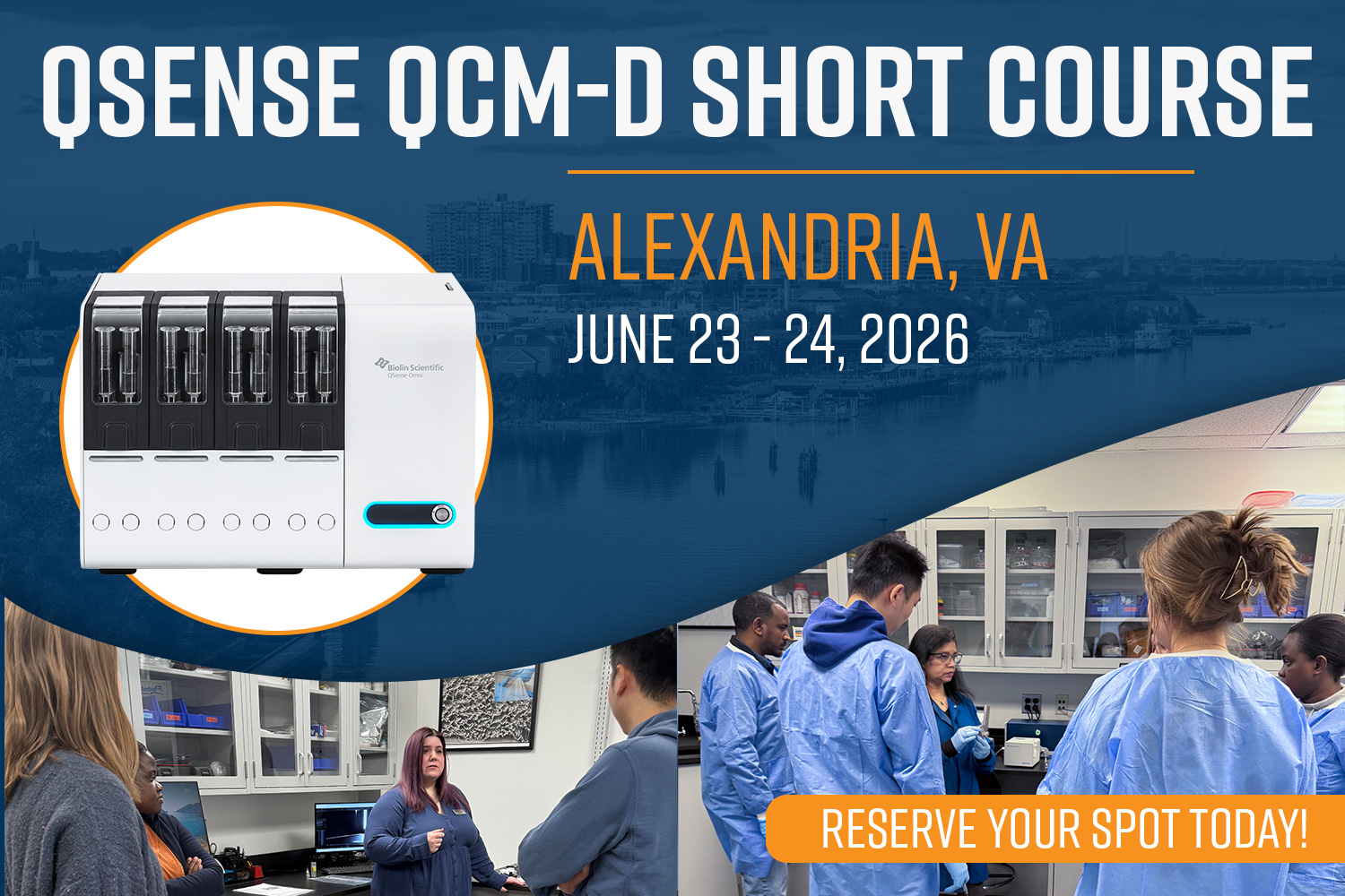
2-Day QCM-D Short Courses: Join our specialized 2-day QCM-D (Quartz-crystal Microbalance with Dissipation monitoring) Short Course. Held in Alexandria, VA, this immersive program is designed…
Posted: April 8, 2026
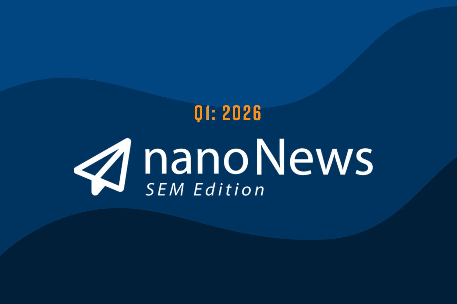
Welcome to the Scanning Electron Microscopy (SEM) edition of the Nanoscience Instruments newsletter, nanoNews! We are excited to share the latest updates from around the…
Posted: April 2, 2026
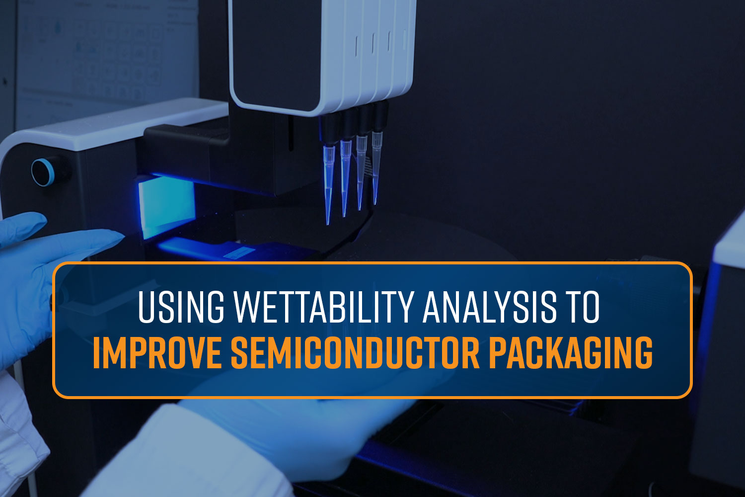
As semiconductor devices continue to shrink and packaging architectures grow more complex, surface interactions play an increasingly important role in overall performance and reliability. Wettability…
Posted: April 1, 2026

Electron Microscopy in Life Sciences There are a number of common electron microscopy methods deployed in life sciences for imaging. The basic entry-level is Scanning…
Posted: March 18, 2026
This site is protected by reCAPTCHA and the Google Privacy Policy and Terms of Service apply.