What is Cathodoluminescence? (CL)
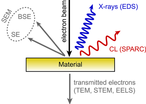
When an electron beam interacts with a material, a multitude of processes occur which are employed for various kinds of microscopy. Besides electron signals, a broad spectrum of electromagnetic radiation ranging from x-rays to the mid-IR is generated through a variety of incoherent and coherent processes.
The radiation that is generated in the ultraviolet/visible/near-infrared regime of the electromagnetic spectrum is referred to as cathodoluminescence (CL), coming from cathode rays (fast electrons) and luminescence (light emission). The electron beam causes the material to fluoresce as it returns to a ground state.
SEM Cathodoluminescence Imaging Microscopy
Cathodoluminescence (CL) is used to characterize optical properties at the nanoscale. Cathodoluminescence techniques analyze the resulting photons that are emitted in the ultraviolet to near-infrared region of the electromagnetic spectrum. The power of cathodoluminescence is the combination of functional optical information with the high spatial resolution of electron microscopy. Cathodoluminescence combines functional optical information with the superior spatial resolution associated with electron microscopy. This makes the technique highly appealing for a large variety of applications and research, especially in the fields of optics research, materials science, and geology.
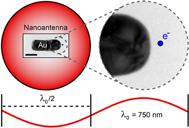
Obtaining optical information on nanostructures with conventional optical microscopy is impossible because optical microscopy is limited in resolution based on Abbe’s law of diffraction. Abbe’s law of diffraction states that two points that are spaced less than d = λ0/(2NA), where λ0 is the free space wavelength and NA is the numerical aperture of the microscope, cannot be resolved by the microscope. With near-ideal numbers, using a blue laser with a λ0 of 400nm and a theoretical perfect NA in air of 1 (although oil immersion apertures can be slightly higher) we are limited to 200nm resolution. This makes conventional optical microscopy unsuited for studies at the true nanoscale.
The above diagram includes an Electron micrograph of a 125 nm long gold rod, which acts as nanoantenna and is resonant at λ0 = 750 nm. The scale bar is 50 nm. The overlaid red circle represents an optical diffraction-limited spot for λ0 = 750 nm and an NA = 1. The small blue dot represents a 5 nm electron beam (to scale). A magnified image of the area enclosed by the gray dashed circle is shown on the right. This image illustrates the limits of optical microscopy and the importance of electron beam excitation for studying nanomaterials.
The solution to this problem is to use cathodoluminescence, a beam of fast electrons to probe materials at the nanoscale. Using electrons as an optical excitation source has several advantages. First, the excitation resolution can be very high and precise. Typical scanning electron microscopes can focus and position an electron beam with 1 – 10 nm. The beam acts as a probeless, and nondestructive broad band excitation source. Since the measurements are performed in an electron microscope environment the full electron microscopy toolbox can be used to correlate nanoscale geometrical features with the optical response.
Cathodoluminescence Applications
Cathodoluminescence emission can be used to explore many fundamental properties of matter. It can be used to study light transport, scattering, electronic structure of materials, including semiconductors, (e.g. bandgap, defects), resonant phenomena and much more. It thus presents a valuable source of information for fundamental research as well as applied research with a direct link to industry (metrology, failure analysis).
A relevant technology in the field of nanophotonics, CL generates hyperspectral light-emission maps that reflect the local density of electromagnetic states. With recent advances in CL, the directionality and polarization of emission can rigorously be measured to provide insight into the optical properties of nanostructures. Until recently CL was not applicable to metallic, dielectric or most semiconductor nanostructures, but breakthroughs in collection efficiency have made CL studies of these structures possible. Improvements in mirror design and alignment have made advanced CL measurements on previously difficult samples, such as nanoparticles, nanowires, metamolecules, metasurfaces, and photonic crystals possible in off-the-shelf systems.
Cathodoluminescence imaging is also an ideal tool to study geological samples. The CL emission from a rock gives insights into crystal growth, zonation, cementation, replacement, deformation, provenance, trace elements, and defect structures. This can be used to fingerprint rocks and reveal interesting spatial textures on a submicron scale. It has proven to be an excellent and non-destructive complement in geochronology to larger and more cumbersome techniques, such as mass spectrometry.
Panchromatic Cathodoluminescence Imaging
A multitude of electron microscope-based imaging techniques exist to provide unique contrasts in materials. Cathodoluminescence (CL) imaging collects and measures the light generated by an electron beam directed at a material. The fastest and simplest method to obtain CL imaging is by performing intensity mapping. This method records the CL intensity for every beam position using a single-pixel light detector.
There are two methods to achieve this: panchromatic and color-filter cathodoluminescence. Panchromatic imaging averages the CL signal over all wavelengths (colors) that fall within the detection range. Color-filtered CL intensity mapping can be performed by introducing a color filter.
Photomultiplier Tube
The SPARC Cathodoluminescence system uses a photomultiplier tube (PMT) light detector in conjunction with a filter wheel. This allows intensity mapping at seven distinct wavelength bands (the 8th entry is empty, allowing panchromatic imaging).
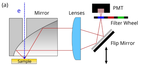
The PMT detector is fast, sensitive, and has a large detection area which allows for fast scanning of large sample areas with high resolution. The pixel dwell times can be as low as 1 µs per pixel, enabling video-rate cathodoluminescence imaging. Areas larger than 0.5 × 0.5 mm can be covered in a single scan making it ideal for scanning larger-scale structures or making CL overview images. This is used to identify regions of interest for more in-depth CL studies (e.g. CL spectroscopy).
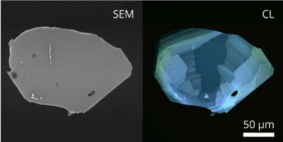
Below is a figure showing a Scanning Electron Microscope image on the left and a Cathodoluminescence measurement on the right. The additional detail on the right was acquired using a PMT and three filters in the blue and green part of the spectrum. These additional details revealed with the CL measurement help in determining details of crystal growth, zonation, defects, and other artifacts of interest.
Hyperspectral Cathodoluminescence Imaging
What is Cathodoluminescence Imaging?
When an electron beam interacts with a material, a spectrum of light can be emitted called cathodoluminescence (CL). The wavelengths that are dominant depends on the local material composition, configuration, and geometry. In panchromatic imaging, the total intensity of all the wavelengths in a range combined is measured. However, much information is lost, as the wavelength distribution (spectrum) often contains valuable information on the local optical and structural properties of the material.
Hyperspectral Imaging Advancements with the SPARC
Wavelength information can be obtained by using color filters, but the scan has to be conducted for each wavelength which is tedious. In hyperspectral imaging, a complete spectrum is collected in a parallel manner providing a high-resolution spectrum for every electron beam position. The CL emission is directed towards a spectrograph containing an optical component with a periodic structure that splits and diffracts light into several beams traveling in different directions. This diffraction grating coupled with a pixelated charge coupled device (CCD), a complementary metal oxide semiconductor (CMOS), or photodiode array spatially disperses the different emission wavelengths over the camera so that each line of pixels corresponds to a unique wavelength.
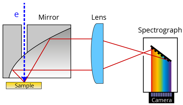
The coupling into the spectrograph can either be through free space, as shown above, or through an optical fiber. Efficient hyperspectral imaging requires a perfect parallel beam from the mirror to the detector, which can only be obtained when the mirror is properly aligned. An ideal example of this is the SPARC system, which uses an advanced micro-positioning system and melt-spun mirror. Without these improvements, light collection efficiency drops by up to 100 times. This means that data acquisition can take 100 times longer or simply becomes impossible because of noise. Detector efficiency is already high enough that further detector improvements cannot physically compensate for these collection losses.
The main parameters for hyperspectral imaging are the wavelength range and resolution. The key components that determine these are the lens system, diffraction grating and detector (camera in the diagram), when combined called a spectrometer. Optical lenses must take chromatic aberration into consideration for systems that can span a large part of the UV to IR spectrum. Chromatic aberration (also known as color fringing or dispersion) is the effect where light at different wavelengths are focused at different distances for the same lens. To focus both UV and IR light from the same source to the same detector the lens configuration must be changed.
With the SPARC, these optics are easily exchanged, the grating and detector work together. The grating needs to be positioned such that it diffracts the spectrum to the detector. The grating determines what wavelengths are diffracted and how wide the pattern is. This determines the spectral resolution. For instance, if you project a 500nm wide spectrum onto 100 linear pixels of a detector, you would have a 5nm spectral resolution, if you changed gratings or geometry and projected only a 50nm wide spectrum onto 100 linear pixels you would have a .5nm spectral resolution. Typical resolutions are 1 to .1nm. The final piece of the puzzle is the detector itself. Detectors have a wide range of response curves that determine their quantum efficiency, or light conversion capability, at different wavelengths.
There are generally no cost-effective detectors with sufficient efficiency for the entire UV to IR range, so often multiple detectors are used, with each specializing in a particular part of the spectrum. Once all of these items are in place entire spectrums can be collected at once from areas of interest on the sample, this is called hyperspectral imaging.
Visualization of Hyperspectral Imaging
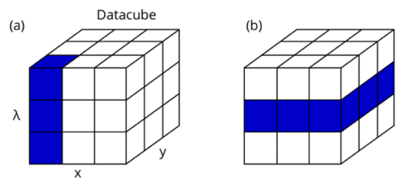
Hyperspectral imaging yields a 3D datacube in which two of the dimensions represent the spatial electron beam position (x,y) and the third represents the wavelength. This datacube is similar to what is collected in EDS or WDS but for UV/VIS/IR wavelengths rather than x-ray wavelengths. The CL datacube contains a wealth of information which can be visualized in many different ways.
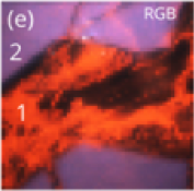
Rather than showing the spectrum for a specific point it is also possible to rigorously visualize spatial differences in the emission for every excitation position. For example, a (false) color RGB image can be extracted from the datacube where the emission spectrum is divided into three RGB channels in a certain spectral range. In this case, we chose the spectral region from 380 to 700 nm which covers both peaks as shown above.
Angle-Resolved Cathodoluminescence Imaging
In cathodoluminescence (CL) imaging the wavelength-dependent intensity (spectrum) is often studied. In addition to the wavelength (color) of the emission, light is also characterized by a wave vector, the momentum and propagation direction of the wave. The direction in which light is emitted contains valuable information on how a nanostructured object emits and scatters light. It is also an important performance metric for plasmonic antenna structures and extracting band structure information from periodic systems, such as photonic crystals.
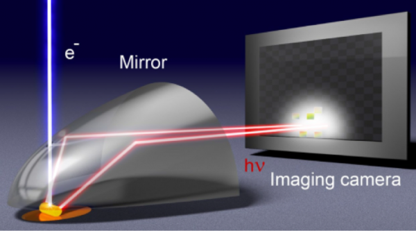
The CL emission is collected by an aluminum paraboloid mirror and redirected out of the SEM chamber toward a 2D CCD or CMOS imaging array in a parallel beam. This allows full retrieval of the beam intensity profile. Shown below is an experimental example of such a profile measured on a single-crystal gold substrate, corrected for mirror geometry. The experiment (on the left) demonstrates the full beam profile and the correlation with the theoretical example (on the right). This example used an SEM to energize the top of a gold nanopillar and measured the angle of the CL radiation coming off of the top of the pillar. In this example, the radiation was toroidal, with little CL signal perpendicular or parallel to the top surface. Every point within this profile can be directly associated with a specific emission angle in the upper angular hemisphere from which CL is collected. Such imaging is also known in optics as ‘Fourier’ imaging, referring to the fact that one image’s momentum (angular) space rather than real space.
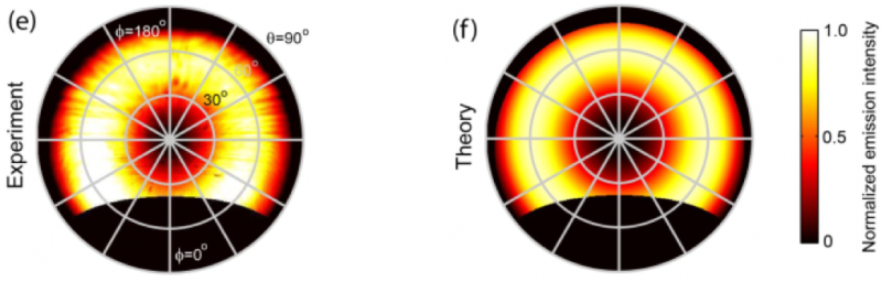
The areas of missing data corresponding to the hole in the top of the mirror (center) and the opening of the mirror to the detector (bottom). The SPARC is the only commercially available solution for angle-resolved CL imaging because of the mirror and its positioning stage housed inside the device. The mirror collects 1.46π steradian of the upper hemisphere of CL emission from the sample. For example, a full sphere is 4π steradian, radiation can only be collected from the top half in an ideal situation, leaving 2π steradian available for collection. Losses from the opening of the mirror towards the detector and for the electron beam, along with the mirror being slightly above the same lead to around a ¼ loss, giving us 1.46π steradian collection area. This is equivalent to a numerical aperture of 0.96, 1.0 being perfect collection in air, and is able to collect zenithal angles up to 88⁰, limited from 90⁰ because of the hole at the top of the mirror for the electron beam The angular profile of gold corresponds to a toroidal pattern because the CL emission is dominated by transition radiation (TR), this angular pattern is shown above, and again, agrees well with theory.
This measurement is not compatible with standard hyperspectral imaging, but color filters can be used to isolate certain spectral ranges since the angular profile can change profoundly for different emission wavelengths. The angle resolve measurements, including angle-resolved combinations with polarizers to study polarization effects, are exclusively available on SPARC as an all-in-one modular device.
Polarization-Filtered Cathodoluminescence Imaging
Light is a transverse electromagnetic wave: the electric and magnetic fields that compose the light wave always oscillate transversely to the propagation direction.
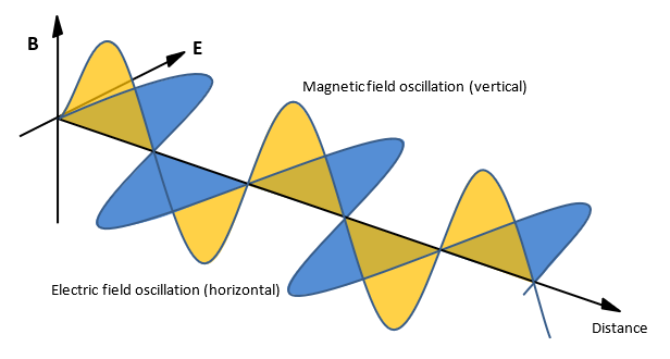
Besides color (energy) and momentum (propagation direction), light is also characterized by a polarization which describes in what direction these electromagnetic fields oscillate. If the electromagnetic oscillations remain in the same plane, the polarization is referred to as linear. This plane can also rotate while the wave is propagating. In that case, the polarization is elliptical which can be either left – (anti-clockwise) or right-handed (clockwise) depending on the direction of rotation (circular polarization is a special case of elliptical polarization).
Angle-Resolved Polarimetry
The figure below is a schematic representation of the angle-resolved polarimetry imaging mode, currently only available on the Delmic SPARC. The cathodoluminescence is collected by the paraboloid mirror and then filtered by the polarization analyzer which consists of a quarter-wave plate (QWP) and a linear polarizer (LP).
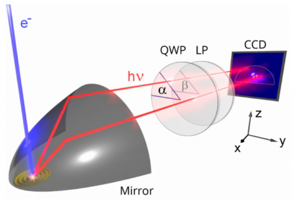
The CCD camera records the polarization filtered image. When images are captured over six different analyzer settings, the full polarization state is retrieved for every emission angle. The original emission of the sample can then be reconstructed by applying a correction for the distorting effect of the paraboloid. This correction is also wavelength dependent, so color filters are used to increase the accuracy of the correction and to achieve spectral sensitivity. It is also possible to perform polarization filtered hyperspectral imaging without angle-resolution. In this imaging modality, it is possible to obtain polarization-filtered nanoscale hyperspectral images. This technique was previously unavailable on commercial systems because it requires very high precision in mirror alignment, a high collection efficiency and a detailed understanding of the mirror distortion.
Polarization Visualization
Polarization plays a key role in light-matter interactions and can be used to study coherence, scattering, birefringence/birefractive, and chirality. Additionally, it can be used to block spurious background radiation and to correct for aberrating effects in the collection optics. When light is emitted from a (nano)material the polarization is not necessarily the same for every emission angle. Fully comprehensive polarization studies have to be performed in the Fourier-plane, otherwise known as angle-resolved mode. The SPARC is the only commercially available tool that can perform angle-resolved imaging to study polarization effects in this manner.
An example of what can be done with this technique is shown in below. This image shows the radial and azimuthal electric field amplitudes for different emission angles on a gold plasmonic bullseye grating, measured with CL polarimetry.
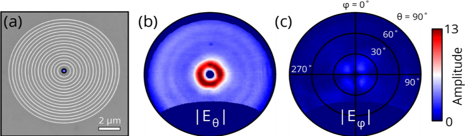
The data above was generated by using an electron beam to launch a circular plasmon wave in the center of the bullseye which is converted by the structure into a radially polarized coaxial beam. The azimuthal component is negligibly small for this geometry. In this case, the light is linearly polarized, but in principle, the handedness can also be determined if the emission is elliptically polarized.