One of the most common challenges when analyzing non-conductive samples with a scanning electron microscope (SEM) is the charging effect. Without a conductive path, the electrons accumulate at the surface, resulting in a distorted image with skewed grayscale values. Although, in some cases, adjusting electron beam parameters and imaging conditions can be sufficient for mitigating charge build-up, sputter coating a conductive layer remains the most effective method for reducing sample charging. Gold and platinum are the most common metals used for sputter coating SEM samples.
In this blog post, we will offer an overview of sputter coating for SEM applications and discuss the different advantages gold and platinum offer to optimize SEM imaging of non-conductive samples.

What is the charging effect?
An SEM operates by scanning a focused electron beam across the surface of a sample. The electron beam interacts with the atoms of the sample, and those interactions produce signals that are detected by specialized detectors to generate an image of a sample’s surface. Charging occurs with non-conductive samples in an SEM because these materials do not readily conduct electricity. When the primary electron beam strikes the surface of a nonconductive sample, it can induce the accumulation of charge on the surface. This charge buildup can distort the trajectory of the electron beam and obscure the signals acquired by the detectors. It can lead to artifacts such as image drift, image distortions, or brightness and contrast artifacts.
How Can Sample Charging be Minimized?
To reduce charging effects, the vacuum level within the SEM chamber can be reduced (an approach known as variable pressure imaging) to allow surface-trapped electrons to dissipate through molecules in the sample chamber. The beam parameters can also be changed to reduce the energy (accelerating voltage) and number of electrons per unit area (beam intensity). However, these changes typically reduce the quality of the image produced by lowering the signal-to-noise and contrast. There is a careful balance between reducing charging and maintaining the highest image quality. An alternative method to reduce charging is by sputter coating the samples with a conductive coating.
What is Sputter Coating?
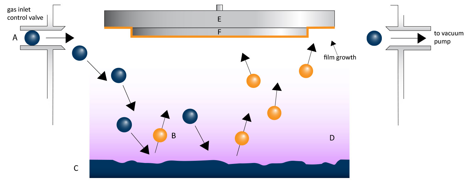
Sputter coating involves applying a thin, uniform layer of conductive material onto a sample. This layer provides electrons with a path to the ground, which reduces charging and improves the quality of the image produced. A sputter coater takes advantage of the principles of gaseous glow discharge between a cathode and an anode (Fig 1). A plasma of suitable gas is generated in the chamber and the cathode target material is bombarded by the gas ions.
The cathode material is ablated and dispersed in all directions, coating any samples placed in the vacuum chamber with an even layer of the target atoms. Gold and platinum are two of the most common materials used as targets, and each offers distinct benefits.
Comparing Low Vacuum Mode vs Conductive Coating for SEM
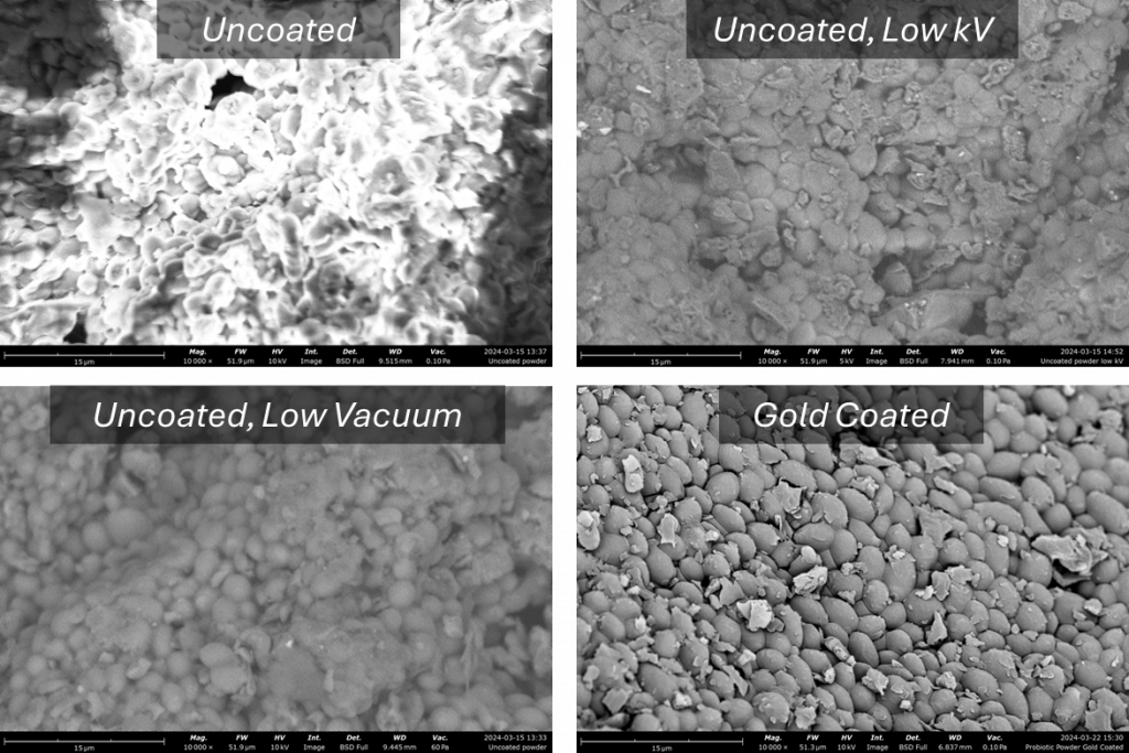
A non-conductive sample, probiotic pharmaceutical powder, was imaged using a Phenom XL Desktop SEM at 10 kV and a vacuum level of 0.1 Pa. At 10,000x magnification typical charging artifacts can be clearly seen (Fig 2A). Reducing the voltage to 5 kV (Fig 2B) or vacuum levels to 60 Pa (Fig 2C) reduces the charging effects but also decreases the amount of signal, leading to a noisier, washed-out image. Under such conditions, obtaining images at higher magnifications would be challenging due to the lack of signal, but also due to the decreasing scan area.
The higher the magnification, the smaller the area over which the beam scans and implants electrons. At a certain point, the path to ground provided by the gas introduced into the sample chamber is no longer sufficient to keep the charge from building up. Coating the sample with gold, thereby adding a conductive layer, enables imaging at higher accelerating voltages and vacuum levels without any charging, resulting in the highest quality image (Fig 2D).
Sputter Coating with Gold
Gold is one of the most popular targets for sputter coating because of its high conductivity and chemical stability. Coating with gold significantly reduces sample charging to allow for crisp, detailed SEM images at low to medium magnification ranges (Fig 2D). Gold sputter coating can be achieved using either air or argon. The typical gold coating grain size is 8-12 nm, which is only revealed when imaging at high magnifications.
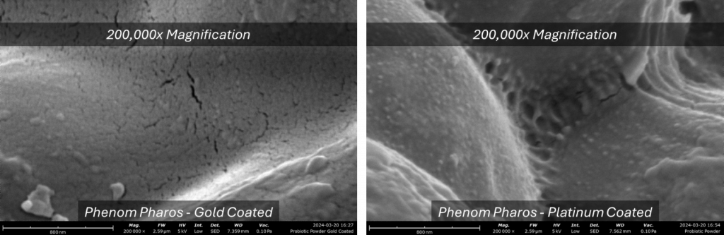
As a rule of thumb, gold coating is optimal when imaging samples with a thermionic emitter electron source as the instrument resolution is typically close to or larger than the grain size. When imaging at higher magnifications using an SEM equipped with a field emission gun (e.g., the Phenom Pharos Desktop SEM), the instrument’s resolution is far less than the gold grain size which results in the appearance of a non-smooth coating that may interfere with the SEM analysis (Fig 3A).
Sputter Coating with Platinum
Platinum is commonly used as a target material for high-magnification applications (>100,000x). Its finer grain size (2-3 nm) improves the resolution of finer surface details compared to gold (Fig 3B). However, platinum is sensitive to stress cracking in the presence of oxygen, so it is recommended to conduct sputter coating in a high-purity gas like argon. Platinum targets also tend to be more expensive than gold, but they deliver far better performance when the features of interest are smaller than 100 nm.
Conclusion
Sputter coating can reduce charging and enable nonconductive samples to be imaged at higher resolution in an SEM by providing a conductive layer on top of the sample. Gold and platinum are two commonly used materials for sputter coating. Coating with gold is beneficial for low to medium-magnification images at an economical price point. Platinum is preferred for acquiring images of sample features smaller than 100 nm.