Charging is one of the most common issues when imaging non-conductive samples by scanning electron microscope (SEM) as it can distort images and damage the sample. Sputter coating samples can significantly improve images produced by an SEM by reducing electron charge build-up. The thin layer of conductive material deposited by sputter coating provides a path for the electrons to travel to the ground.

Determining Coating Thickness
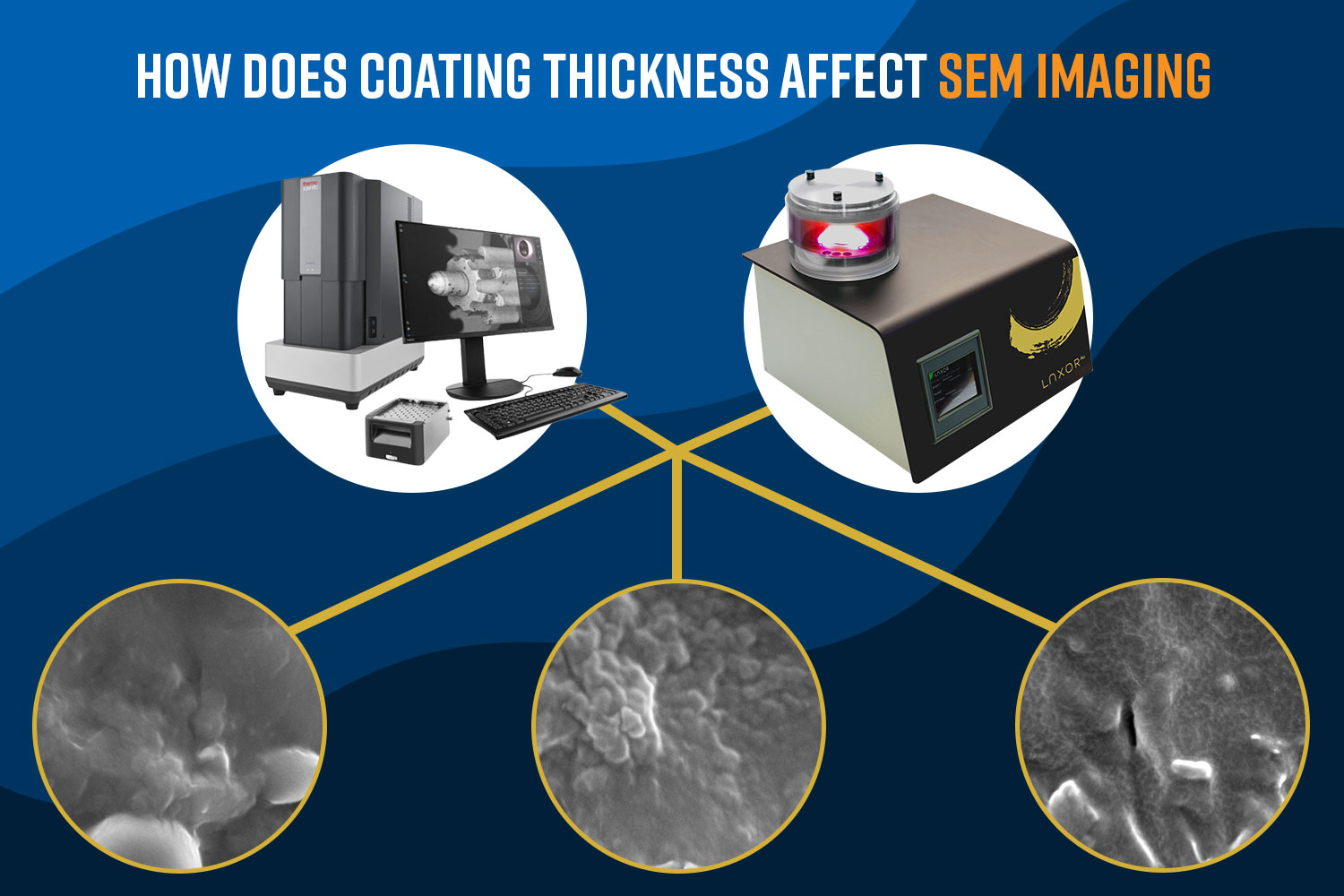
Although sputter coating can significantly improve an SEM image, it can be not easy to decide the thickness of the metallic coating to apply to a sample. A thick enough coating is necessary to ensure that the electrons effectively travel to the ground and reduce charging artifacts while imaging. Thin coatings could end up with small cracks or gaps, effectively adding electrical shorts to their path to the ground. But if the thickness to too large, then it could interfere with the quality of the image.
Optimal coating thickness varies depending on the sample, the intent of the analysis, and the material being used to coat the sample. This blog aims to provide some insight into selecting the right sputter coating thickness to improve the quality of SEM data acquired.


The coating needs to be thick enough to provide a conductive path for electrons to dissipate, but not too much as to decrease the quality of the image, as seen in Figure 1. When 2 nm of gold is applied (Fig 1A), electrons still build up charge in the non-conductive material. 10 nm of gold provides a sufficient path for the electrons to dissipate and produces a quality image (Fig 1B). However, when 25 nm of gold is applied (Fig 1C), the elemental contrast between the particulates and the fibers is dulled, which reduces the amount of information obtained from the image.
In another example, an uncoated sample of rubber showed severe charging effects even at low magnifications (Fig 2A). When coated with 2 nm of gold (Fig 2B), high magnification imaging is possible but slight charging still produces image distortions. When 10 nm of gold was applied (Fig 2D), bumpy features can be seen due to excessive gold coating. The best image was obtained with 6 nm of gold (Fig 2C).


Benefits of Coating a Thin Layer
While it is important to ensure enough coating is applied to complete a conductive path to ground, too much sputter coating can also decrease the quality of an image. Figure 3 shows a surface of coated glass that was imaged using Phenom Pharos, where the surface features are visible. However, coating this surface with 10 nm of gold, masks these features and shows a much smoother surface. In this case, a thinner coating should be used.


When generating elemental contrast with the backscatter detector (BSD), a thinner sputter coating thickness is beneficial as it will preserve the elemental difference. In the example in Figure 4, SEM images of a sample containing both carbon and aluminum particles show a clear contrast in BSD signal when coated with only a couple of nanometers of gold. However, the contrast is significantly reduced when a thicker gold coating is applied.


In addition to visually separating elements, a thinner layer of gold is also beneficial when analyzing materials for their elemental compositions with energy dispersive spectroscopy (EDS). The thicker a metallic coating is, the fewer x-rays are generated by the sample itself rather than from the coating. As coating thickness increases, the characteristic peaks of the sputtered metal increase while the peaks from the sample elements decrease. This is particularly problematic when quantifying low abundance elements or those with peaks near those of the coating as those signals will be overwhelmed by the signals coming from the coating.
Benefits of Coating a Thick Layer
Metallic coating adds a higher-density element to the surface of the sample, which decreases the depth that the beam electrons travel into the sample. Decreasing the depth to which the beam electrons penetrate the sample improves the imaging performance of beam-sensitive samples. As the electron beam interacts with beam-sensitive samples, the sample atoms readily deform, which can negatively impact the image. Sufficiently thick coatings minimize the deformation of the sample atoms, ensuring that high-resolution images can be obtained of the sample surface. To illustrate this, a piece of Teflon tape was imaged using Phenom XL. Uncoated samples show a charging effect (Fig 5A) while coating with 7 nm of Pt eliminates the charging effect but shows significant damage to the sample (Fig 5B). Increasing the coating thickness to 15 nm results in obtaining good high-resolution images (Fig 5C).


Conclusion
Sputter coating can significantly improve the quality of the SEM images, but the correct thickness is key to optimizing the benefit of the coating. Finding that balance point depends on the sample composition and the information extracted from it.
In general, thicker coatings offer:
- Better conductive path for the electrons thereby reducing the charging effect.
- Increased signal.
- Decreased deformation of beam-sensitive samples.
The advantages of thinner coatings include:
- Reduces the chance of covering up smaller surface features.
- Maintains elemental contrast with the BSD.
- Minimizes impact on EDS spectra.