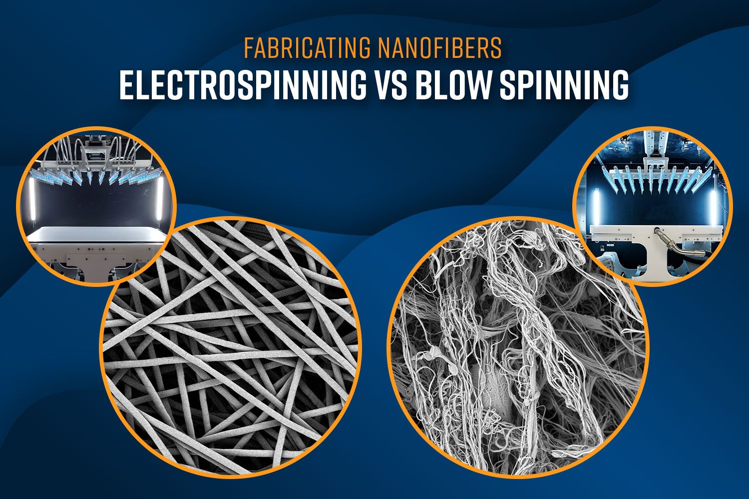
Nanofibers, with their high surface area-to-volume ratio, tunable porosity, and mechanical flexibility, are increasingly used in diverse applications including filtration, biomedical devices, energy storage, and…
Posted: July 9, 2025 | Technology: Electrospinning & Electrospraying
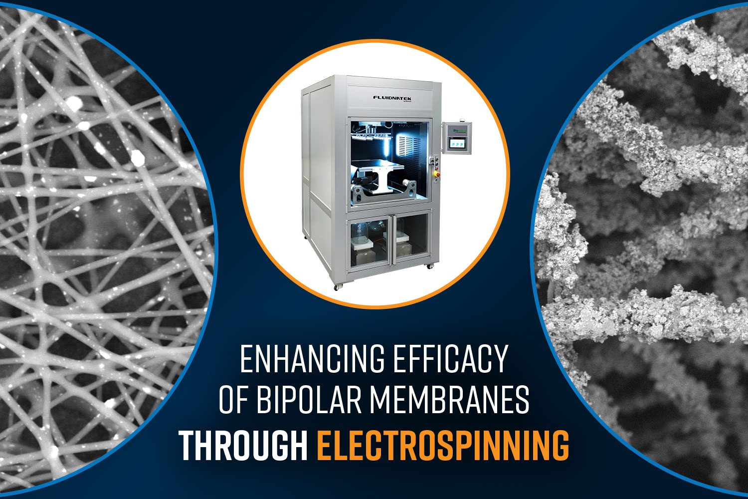
Electrospinning has emerged as a transformative technique for fabricating fibrous materials with highly controlled geometries. This method, characterized by its ability to produce ultrafine fibers…
Posted: June 25, 2025 | Technology: Electrospinning & Electrospraying

Understanding molecular interactions at surfaces is essential for advancing fields such as biosensing, materials science, and drug discovery. These interactions—ranging from protein-ligand binding to polymer…
Posted: June 11, 2025 | Technology: QCM-D
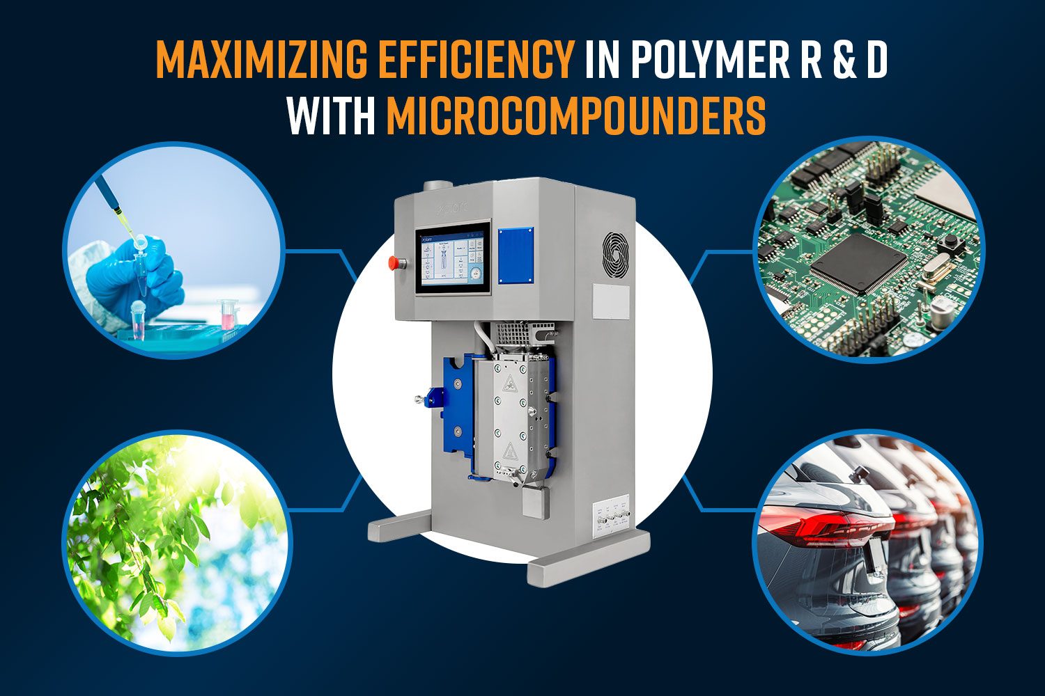
In polymer processing and material research, achieving uniform dispersion and distribution of additives and precise formulation control is crucial for developing advanced materials. This is…
Posted: May 14, 2025 | Technology: Polymer Compounding
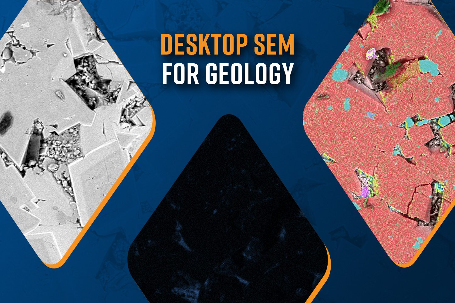
Scanning Electron Microscopy (SEM) is a versatile tool in geology used in high-resolution imaging and chemical analysis of rocks, minerals, and microfossils. SEM provides detailed…
Posted: May 7, 2025 | Technology: Scanning Electron Microscopy
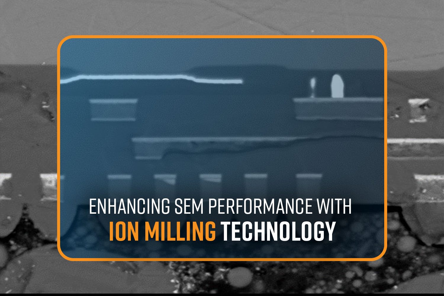
In material science, cross-section polishing is a critical method to enable the detailed examination of a sample material’s microstructure. This technique is essential for understanding…
Posted: April 30, 2025 | Technology: Scanning Electron Microscopy
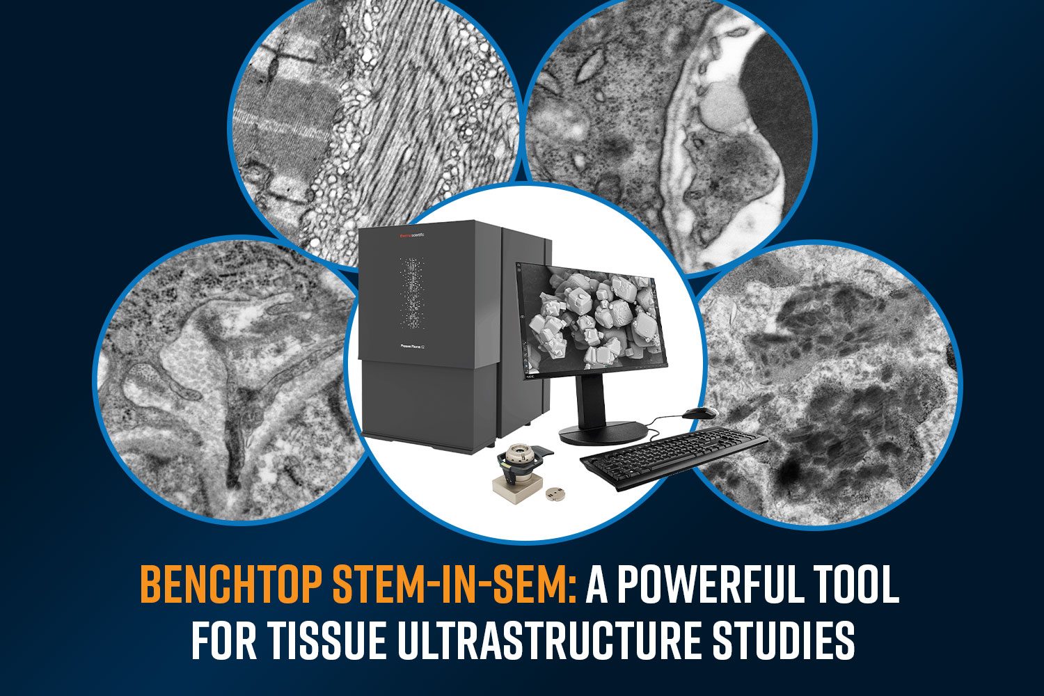
Understanding the ultrastructure of biological tissues is essential for advancing medical research, disease diagnostics, and drug development. Traditionally, histological techniques such as optical microscopy have…
Posted: April 23, 2025 | Technology: STEM, Scanning Electron Microscopy
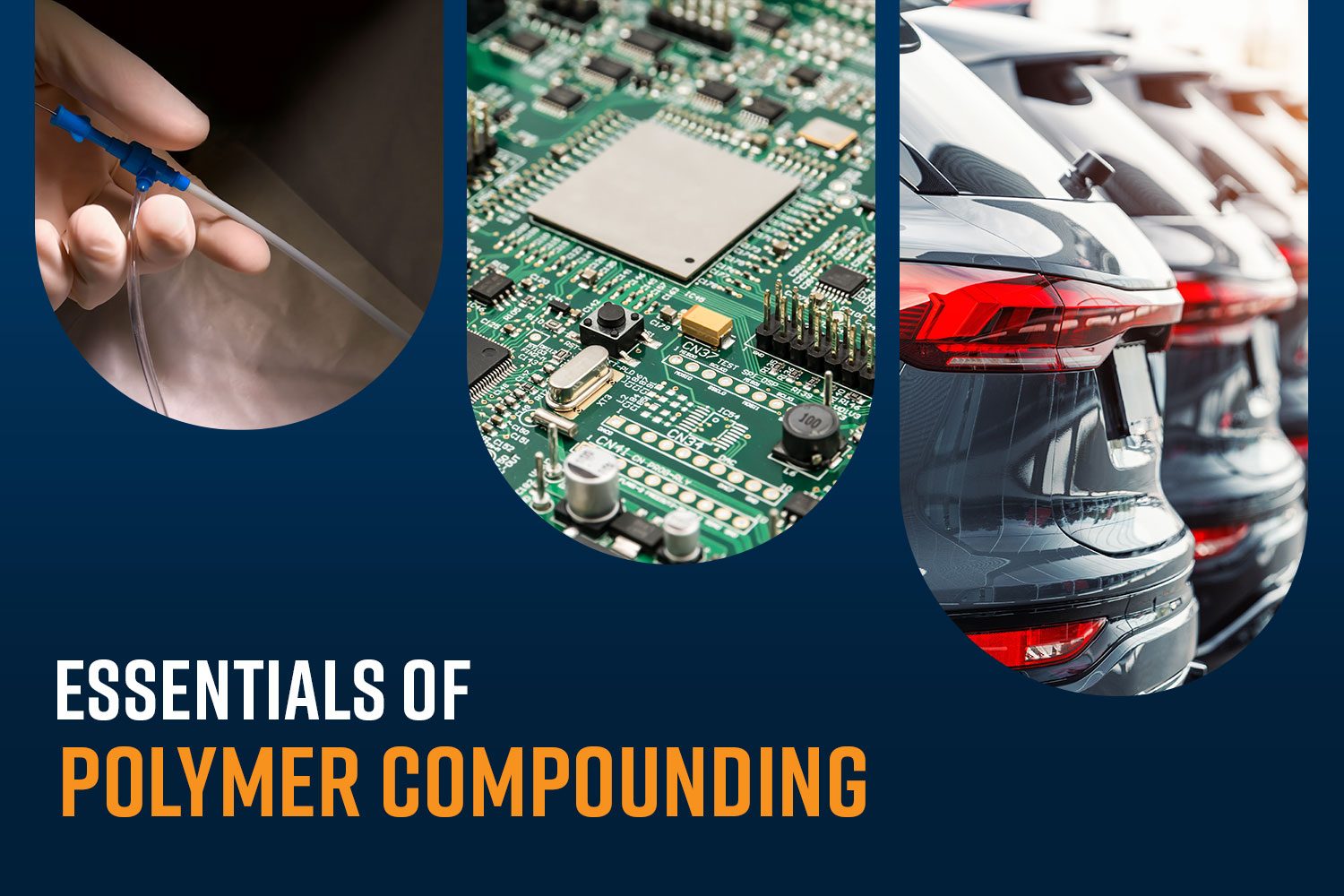
Polymer compounding is a fundamental process in materials engineering that involves blending polymers with various additives to enhance their properties and performance. This allows manufacturers…
Posted: April 16, 2025 | Technology: Polymer Compounding

Particle analysis involves characterizing the size, morphology, and composition of powders and particulate matter to describe their properties in a precise and statistically significant manner….
Posted: April 9, 2025 | Technology: Scanning Electron Microscopy
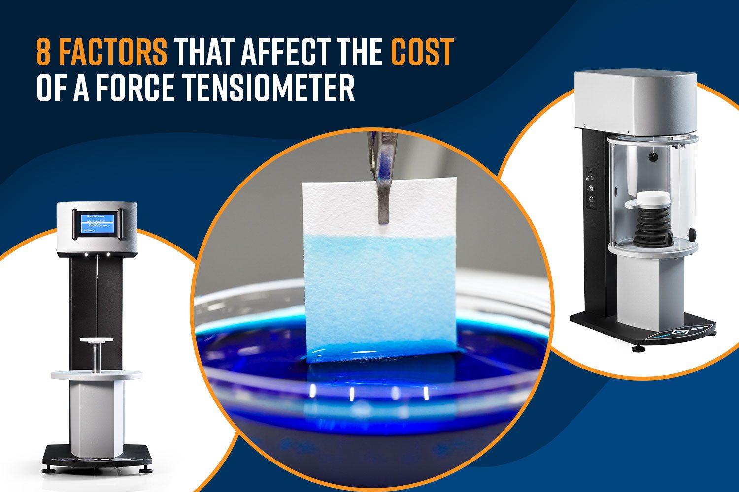
A force tensiometer is an instrument that uses a highly sensitive analytical balance and specialized probes to characterize several key interfacial properties. Even though it…
Posted: April 2, 2025 | Technology: Tensiometry

Cryo-electron microscopy (cryo-EM) is a powerful imaging technique used to determine the structure of biological macromolecules, viruses, and cellular components at near-atomic resolution. Unlike traditional…
Posted: March 26, 2025 | Technology: STEM, Scanning Electron Microscopy

Quartz Crystal Microbalance with Dissipation monitoring (QCM-D) has revolutionized surface science by enabling real-time analysis of molecular interactions. However, traditional QCM-D workflows often involve time-consuming…
Posted: March 19, 2025 | Technology: QCM-D