This fourth quarter Electrospinning edition is packed with new blogs, webinars, and videos. From demonstrating the formation and control of the Taylor cone to a…
Posted: January 3, 2025
We’re pleased to share the latest edition of nanoNews! In the third quarter newsletter, you’ll find our webinar resources, event news, and our newest articles…
Posted: December 31, 2024
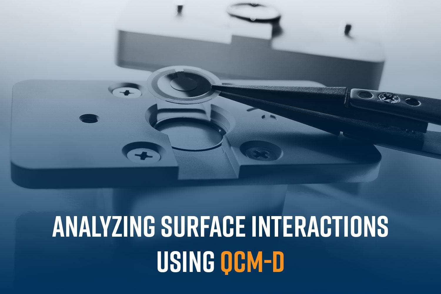
Quartz Crystal Microbalance with Dissipation Monitoring (QCM-D) is a versatile analytical technique that can provide real-time, quantitative data on mass changes and viscoelastic properties of…
Posted: December 18, 2024
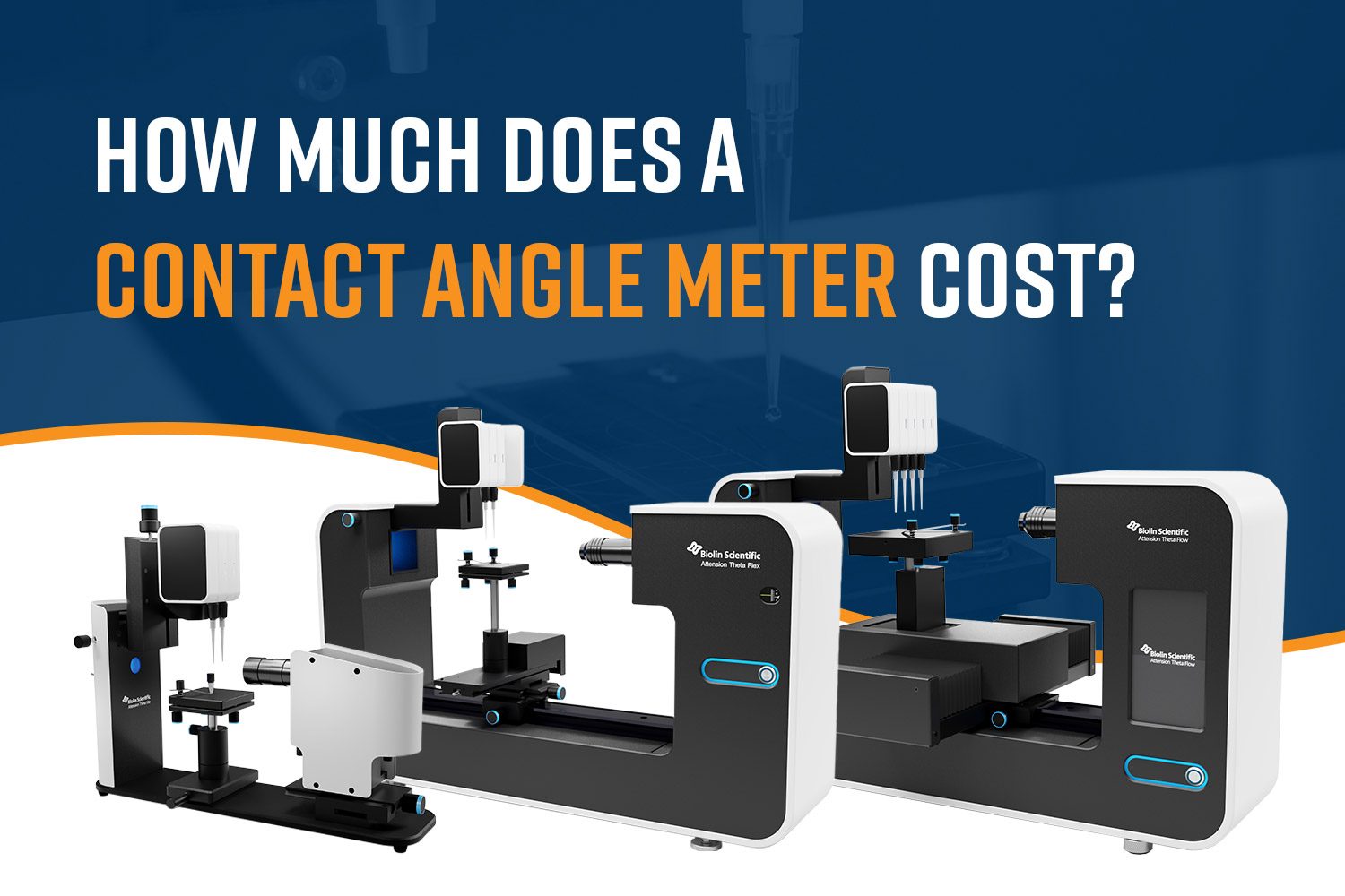
Optical tensiometers, also referred to as goniometers, drop shape analyzers, or contact angle meters, are indispensable instruments used in scientific and industrial applications requiring precise…
Posted: December 11, 2024
MD&M West – Medical Design & Manufacturing West Nanoscience Instruments and our sister company, Nanoscience Analytical, provide cutting-edge instrumentation and process development services to enhance…
Posted: December 11, 2024
In the world of material fabrication, various techniques have emerged to create complex and functional materials for a wide range of applications, from medical devices…
Posted: December 4, 2024
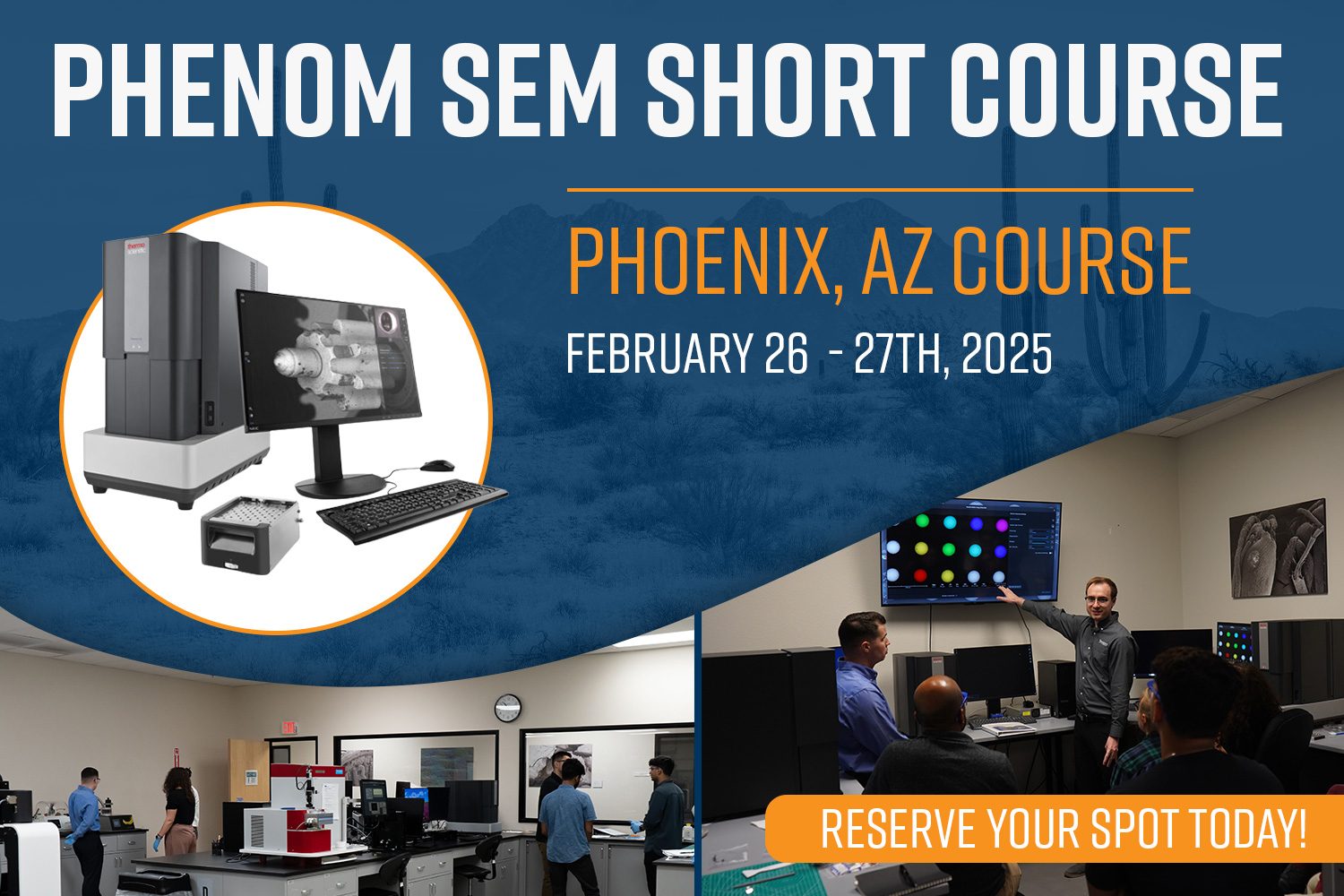
Explore the microscopic world in our specialized 2-day Scanning Electron Microscopy (SEM) Short Course. Held in Phoenix, AZ, this immersive program is designed for both…
Posted: November 25, 2024
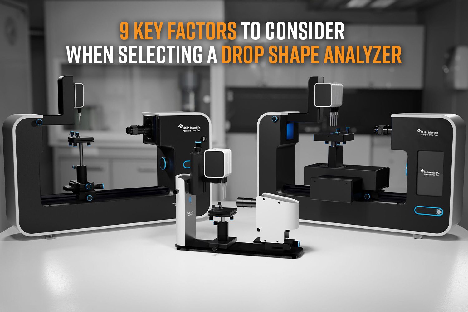
Optical tensiometers, also referred to as goniometers, contact angle meters, or drop shape analyzers, are essential tools in materials science, enabling precise measurements of surface…
Posted: November 20, 2024
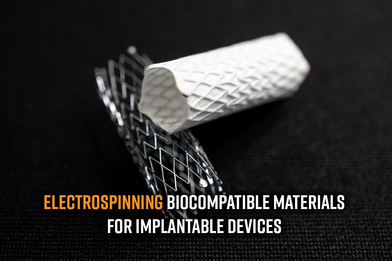
The need for implantable devices and biocompatible materials is driven by the demand for advanced medical solutions that can repair, replace, or support damaged tissues…
Posted: November 13, 2024
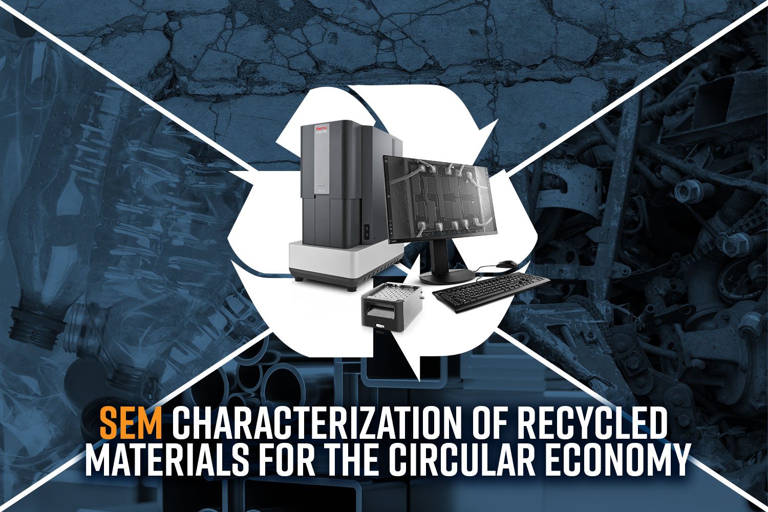
In the age of climate change and resource depletion, the circular economy is increasingly gaining attention. It promotes the reuse, recycling, and repurposing of materials…
Posted: November 6, 2024
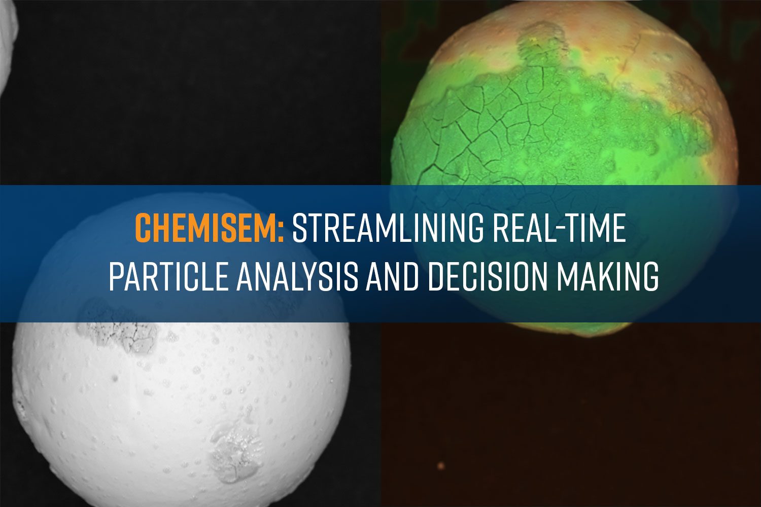
Energy dispersive spectroscopy (EDS) is a microanalysis technique that provides localized elemental composition data, typically used in conjunction with scanning electron microscopy (SEM). While SEM-EDS…
Posted: October 30, 2024
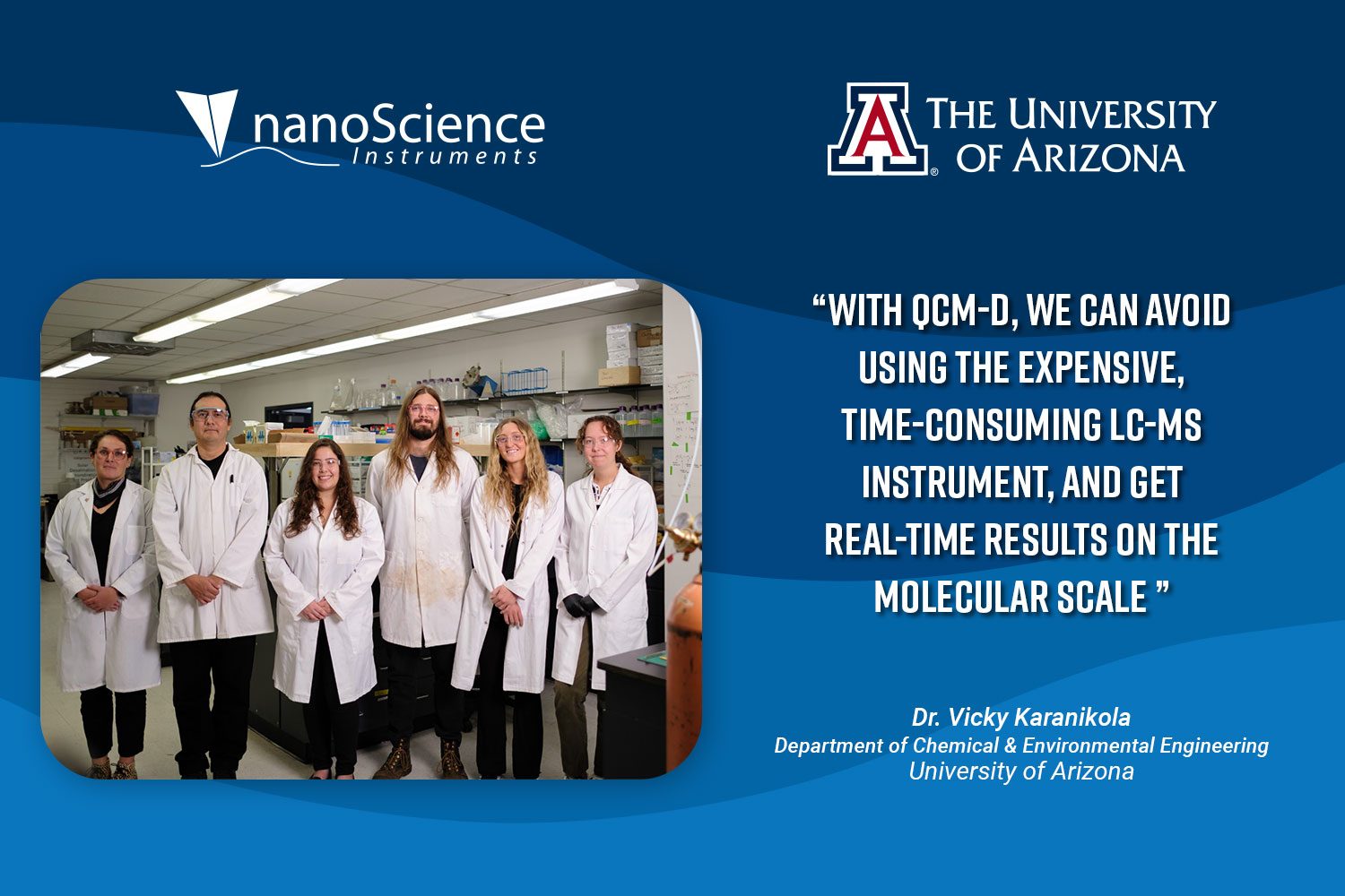
In the KORES (Karanikola Optimized Research for Environmental Sustainability) lab led by Dr. Vicky Karanikola, at the Department of Chemical & Environmental Engineering at the…
Posted: October 25, 2024
Copyright 2025. Nanoscience Instruments. All Rights Reserved.
This site is protected by reCAPTCHA and the Google Privacy Policy and Terms of Service apply.