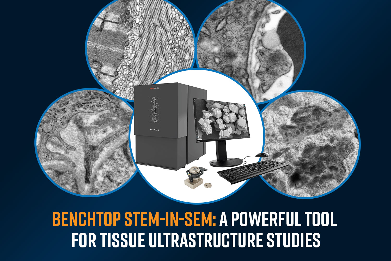
Understanding the ultrastructure of biological tissues is essential for advancing medical research, disease diagnostics, and drug development. Traditionally, histological techniques such as optical microscopy have…
Posted: April 23, 2025
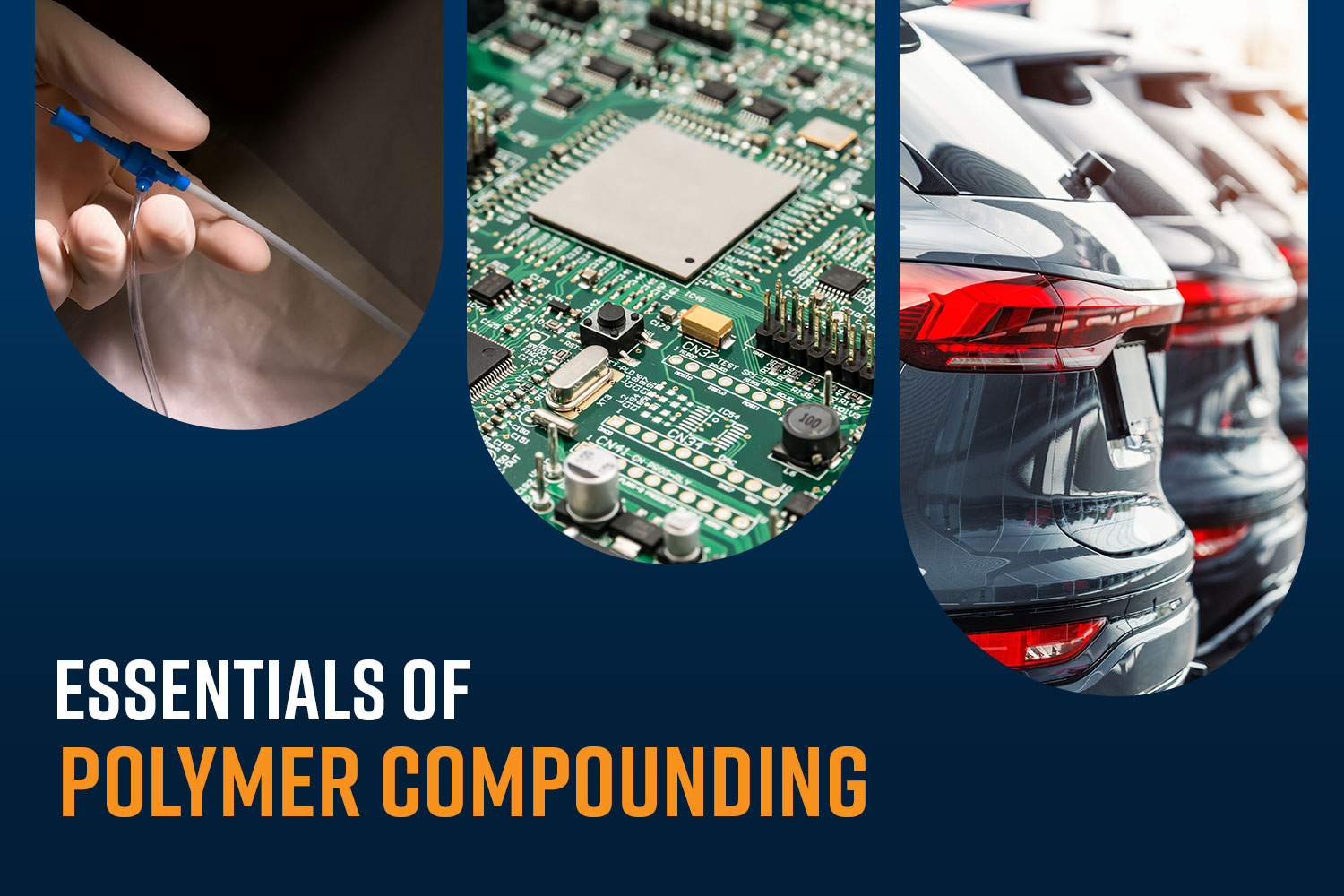
Polymer compounding is a fundamental process in materials engineering that involves blending polymers with various additives to enhance their properties and performance. This allows manufacturers…
Posted: April 16, 2025
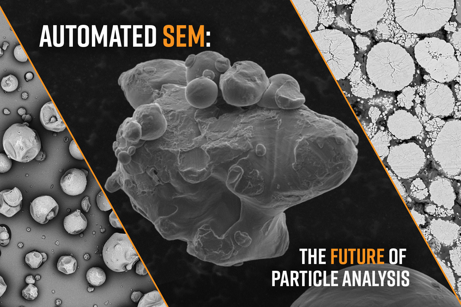
Particle analysis involves characterizing the size, morphology, and composition of powders and particulate matter to describe their properties in a precise and statistically significant manner….
Posted: April 9, 2025
We’re pleased to share the latest edition of nanoNews! In the first quarter of the 2025 newsletter, you’ll find our webinar resources, event news, and…
Posted: April 2, 2025

Association for Iron & Steel Technology Conference 2025 At Nanoscience Instruments, we empower steelmakers by equipping them with the means to achieve comprehensive inclusion analysis…
Posted: April 2, 2025
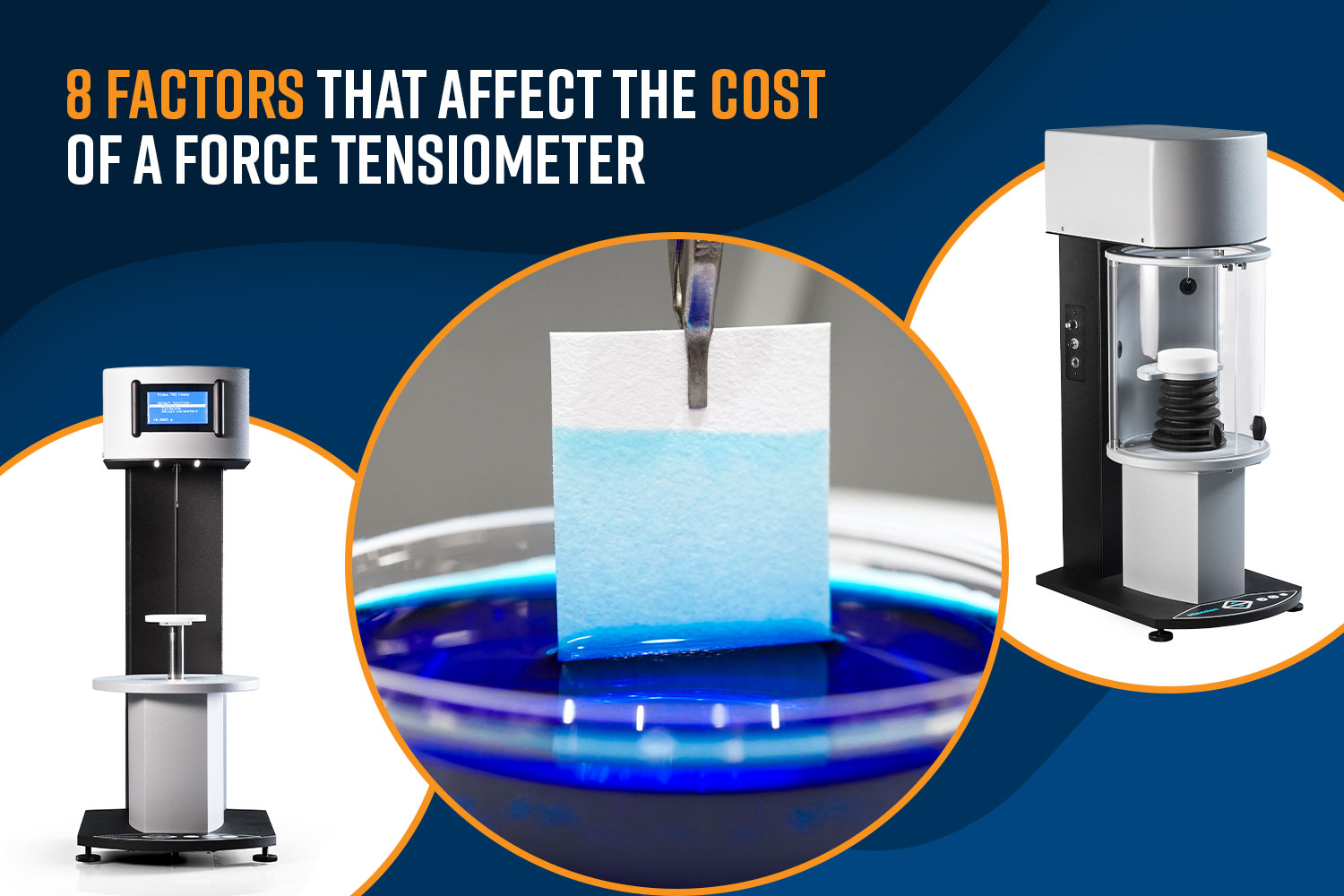
A force tensiometer is an instrument that uses a highly sensitive analytical balance and specialized probes to characterize several key interfacial properties. Even though it…
Posted: April 2, 2025
Cryo-electron microscopy (cryo-EM) is a powerful imaging technique used to determine the structure of biological macromolecules, viruses, and cellular components at near-atomic resolution. Unlike traditional…
Posted: March 26, 2025

Quartz Crystal Microbalance with Dissipation monitoring (QCM-D) has revolutionized surface science by enabling real-time analysis of molecular interactions. However, traditional QCM-D workflows often involve time-consuming…
Posted: March 19, 2025

Nanoscience Instruments provides solutions for battery development applications through cutting-edge instrumentation and analytical services. Visit our booth for live demonstrations of desktop SEM with automated…
Posted: March 18, 2025
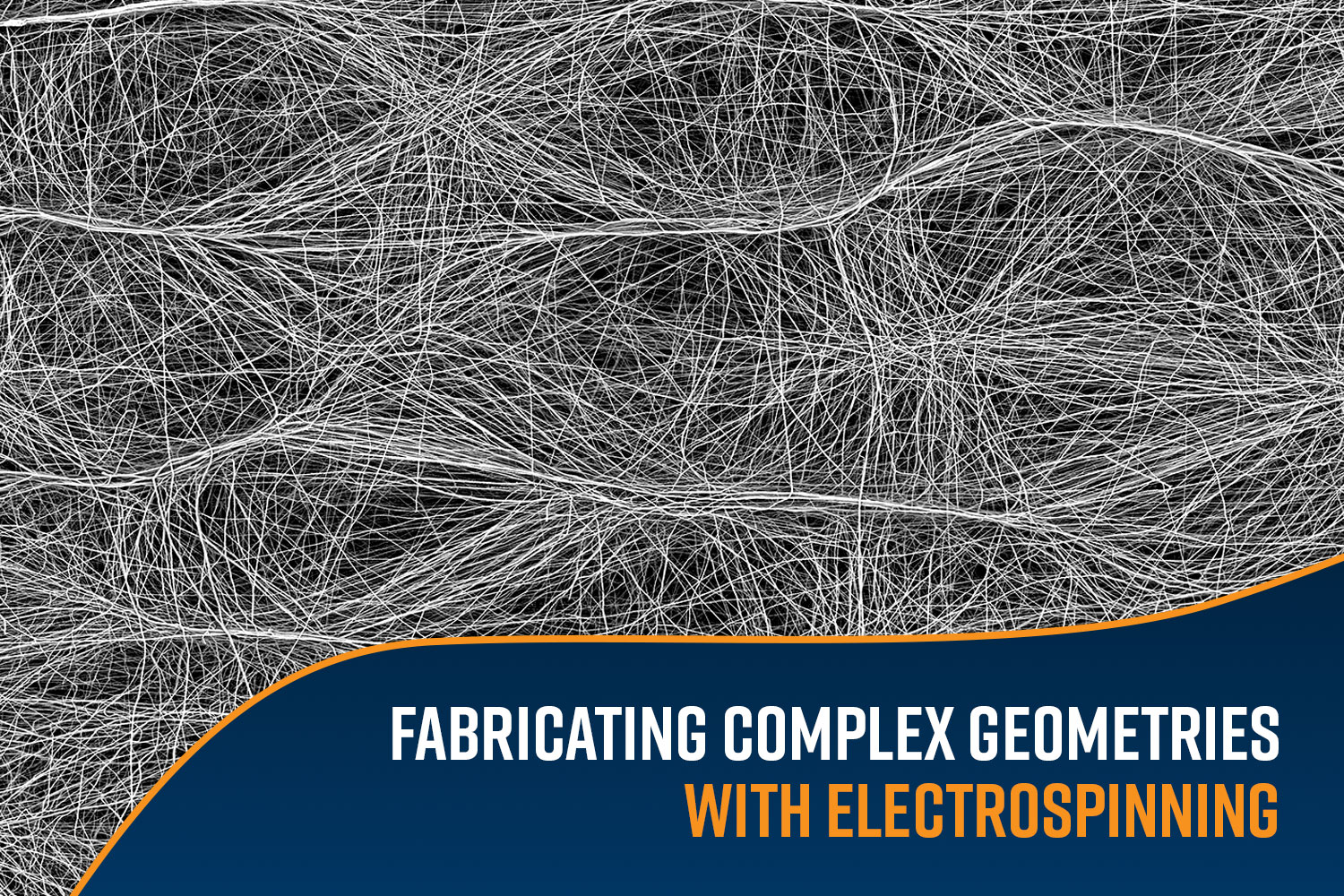
Electrospinning has emerged as a transformative technique for fabricating fibrous materials with highly controlled geometries. This method, characterized by its ability to produce ultrafine fibers…
Posted: March 12, 2025

Particle analysis is a critical process in many industries, from pharmaceutical formulation and nanomaterials development to forensic investigations and industrial manufacturing. Understanding the size, shape,…
Posted: March 5, 2025

Interactions at surfaces and interfaces are crucial in many fields, including environmental science, biopharmaceutical research, materials science, catalysis, and nanotechnology. The ability to detect minute…
Posted: February 26, 2025