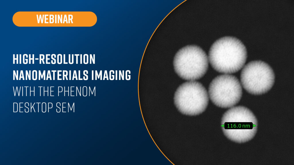
The term “nanomaterials” covers a broad range of inorganic material types, with the common feature between them being their extremely small physical size. This size range typically spans from approximately 1 to 100 nm. Acquiring scanning electron microscope (SEM), scanning transmission electron microscope (STEM) or transmission electron microscope (TEM) images of materials at this scale presents unique challenges related to resolution, signal generation, and beam–sample interactions. However, with proper sample preparation, optimized electron beam parameters, and thoughtful selection of imaging detectors, it is possible to reliably capture high-quality images of nanoscale features.
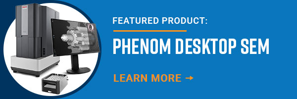
This webinar focuses on practical, tested approaches for imaging nanomaterials using Phenom desktop SEM systems. Attendees will be shown sample preparation methods that improve nanoscale visibility for both SEM and STEM-style imaging workflows. The session will also compare detector choices (SEM: BSD and SED; STEM: BF, DF, and HAADF) and discuss how each mode affects contrast, feature interpretation, and image quality for a variety of nanomaterial types.
In addition, we will examine how accelerating voltage and beam intensity influence resolution, contrast, and signal stability when working in the nanometer regime. All example images and datasets presented in this webinar are collected using Phenom desktop SEM platforms, including data acquired with the accessory STEM detector. While the webinar focuses on desktop instrumentation, the principles discussed can be applied to nearly any SEM or TEM system.