Scanning Transmission Electron Microscopy (STEM) is a scanning-based imaging technique that uses a focused electron beam to raster scan across an ultra-thin sample, typically <150 nm. Although STEM is similar to Scanning Electron Microscopy (SEM), it differs fundamentally in how electrons interact with the sample and how signals are generated (comparison shown in Table 1). Understanding these differences is critical for selecting the appropriate technique for characterization, failure analysis, or research workflows in a range of fields including materials science and life sciences.
| Aspect | STEM | SEM |
| Imaging Principle | Transmitted electrons through sample | Emitted electrons from surface |
| Sample Thickness | Ultra-thin (<100 nm) | Bulk samples |
| Resolution | Sub nanometer scale | Nanometer-scale |
| Information Type | Internal structure, crystallography, atomic contrast | Surface morphology, composition |
| Detectors | BF, DF, HAADF | SE, BSE, EDS |
What is STEM Imaging?
STEM Imaging Principles:
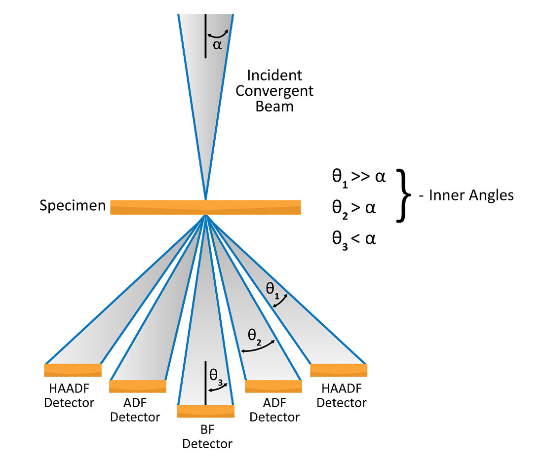
Scanning Transmission Electron Microscopy (STEM) is an imaging mode in which a finely focused electron probe is raster scanned across a thin, electron-transparent sample.1 As electrons transmit through the specimen, they interact with its internal structure and are scattered over a range of angles. These transmitted and scattered electrons are collected by detectors positioned to capture specific angular ranges, forming the basis of different STEM imaging modes (Figure 1).
- Bright Field (BF) detectors collect low-angle, on-axis transmitted electrons
- Dark Field (DF) detectors capture electrons scattered to intermediate angles
- High-Angle Annular Dark Field (HAADF) detectors collect electrons scattered to high angles, producing contrast that scales strongly with atomic number (Z-contrast)
What Does Each STEM Mode Reveal About Your Sample?
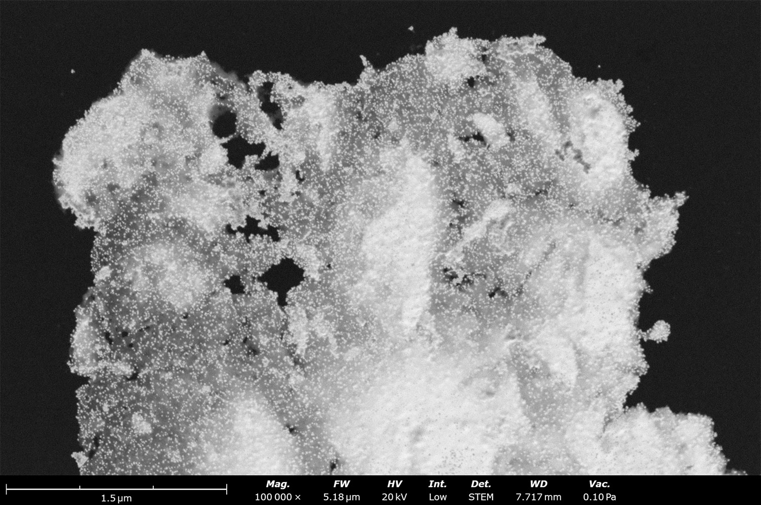
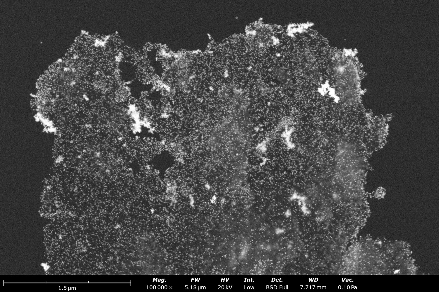
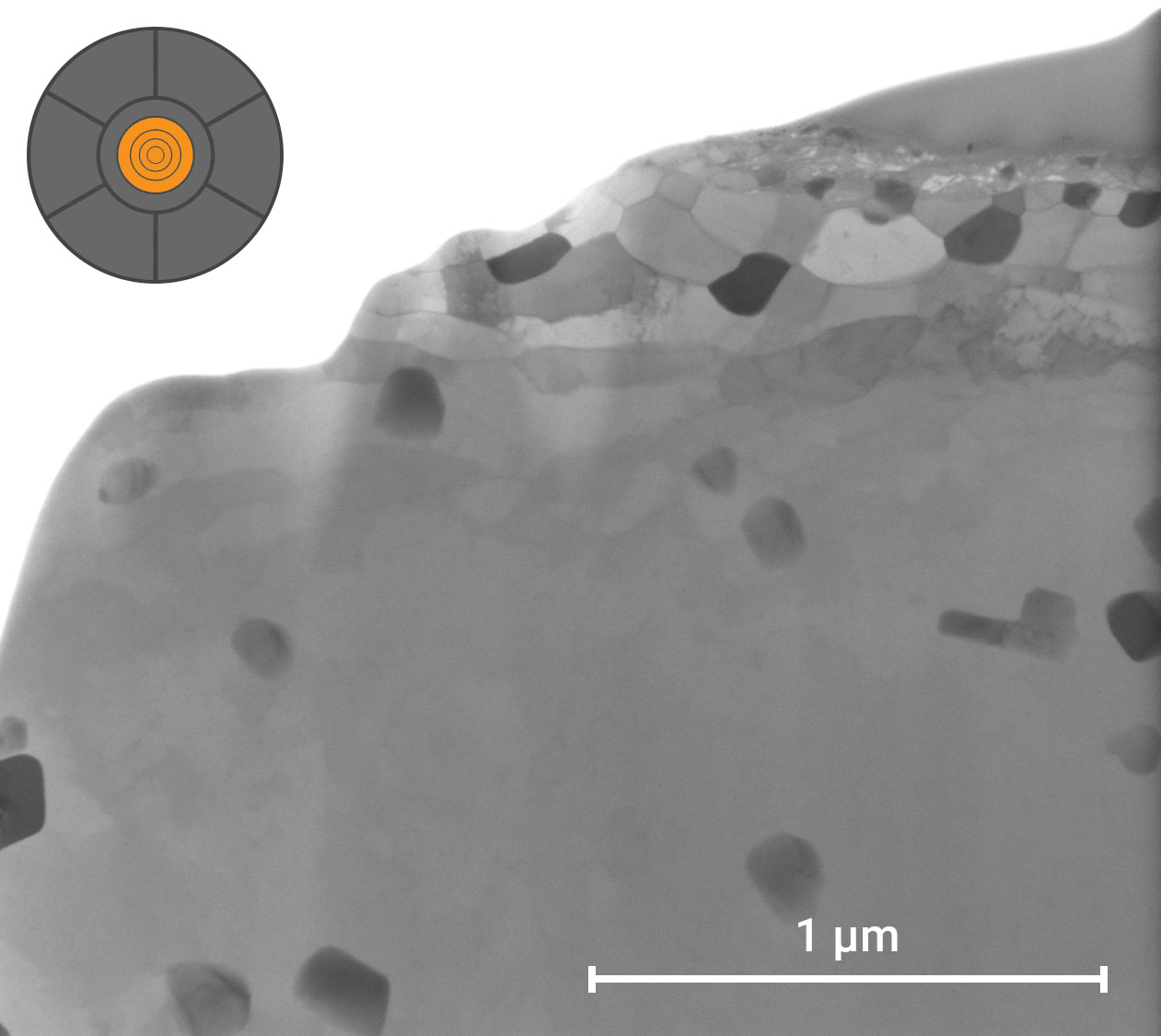
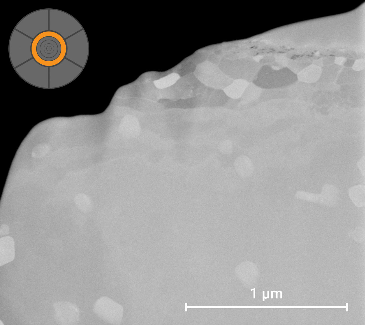
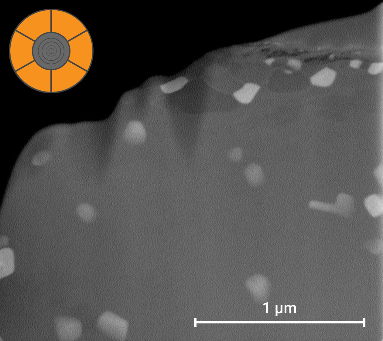
BF, DF, and HAADF imaging modes (shown in Figure 2) each provide distinct and complementary contrast mechanisms, enabling a comprehensive understanding of structure, composition, and morphology.
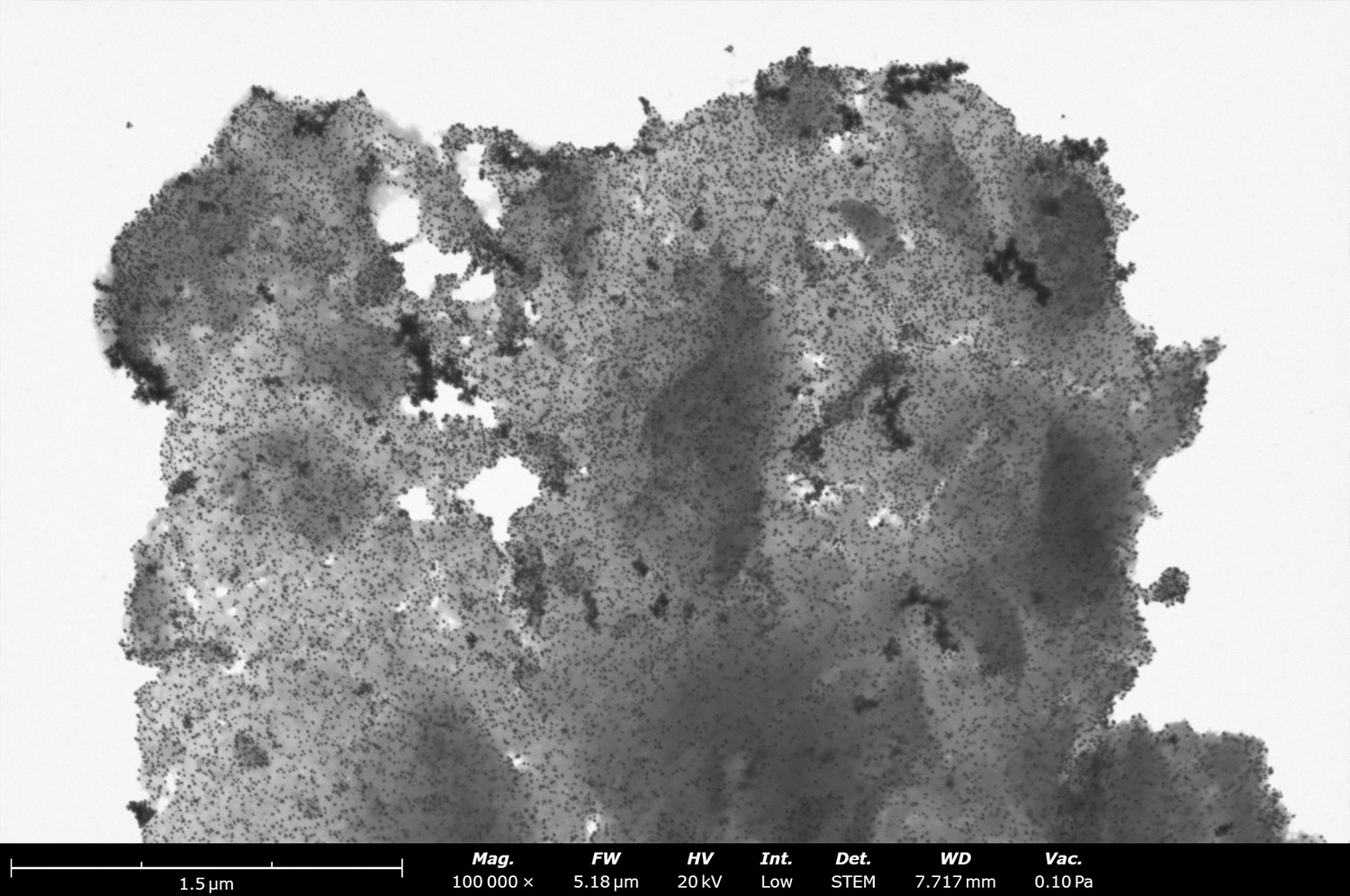
Bright Field: Structural Clarity
BF-STEM (Figure 2a) collects low-angle electrons that pass through the sample with minimal scattering. This mode delivers the highest spatial resolution and is particularly well suited for imaging fine structural details in thin specimens. The contrast arises primarily from mass-thickness and scattering effects with thicker or denser regions appearing darker. It is ideal for visualizing internal morphology, grain boundaries and porosity, and nanoscale features.
Dark Field: Enhanced Feature Visibility
DF-STEM (Figure 2b) captures electrons scattered to intermediate angles, enhancing contrast from features that may be difficult to resolve in BF mode. It improves visibility in heterogeneous or low-contrast materials and highlights structural variations and defects. This mode is particularly useful for identifying small particles, revealing weakly scattering features, and differentiating phases with subtle contrast differences.
High-Angle Annular Dark Field: Compositional Insight (Z-Contrast)
HAADF-STEM (Figure 2c) collects electrons scattered to high angles, where scattering intensity scales strongly with atomic number. It produces Z-contrast imaging with heavier elements appearing brighter. It is effective for identifying compositional variations, locating heavy nanoparticles in lighter matrices, and analyzing multi-material nanoscale systems
How Can You Access STEM Data in a Benchtop System?
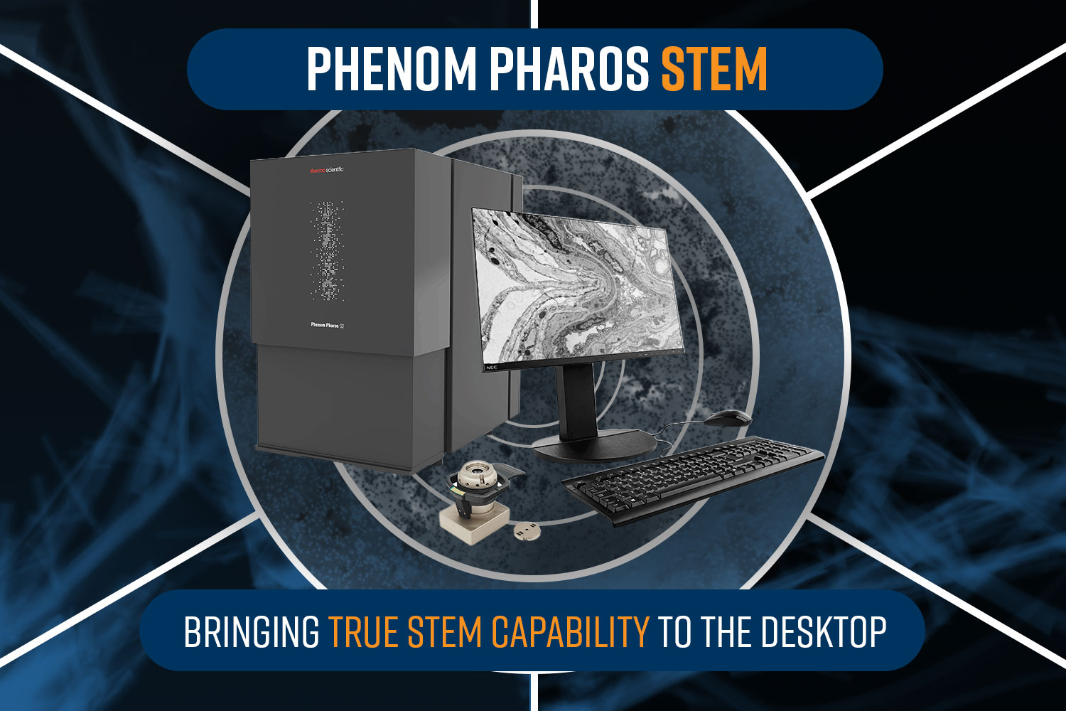
Phenom Pharos Desktop STEM:
The Phenom Pharos Desktop STEM (Figure 3) is a hybrid SEM–STEM platform that integrates transmission imaging capabilities into a compact, user-friendly desktop system, effectively bridging the gap between conventional SEM and full-scale TEM. It combines a field emission gun (FEG) source, an integrated segmented STEM detector, and intuitive software to deliver sub-nanometer (<1 nm) STEM resolution alongside standard SEM functionality. Key STEM features include Bright Field (BF), Dark Field (DF), and High-Angle Annular Dark Field (HAADF) imaging modes, enabling both structural and compositional contrast from electron-transparent samples.
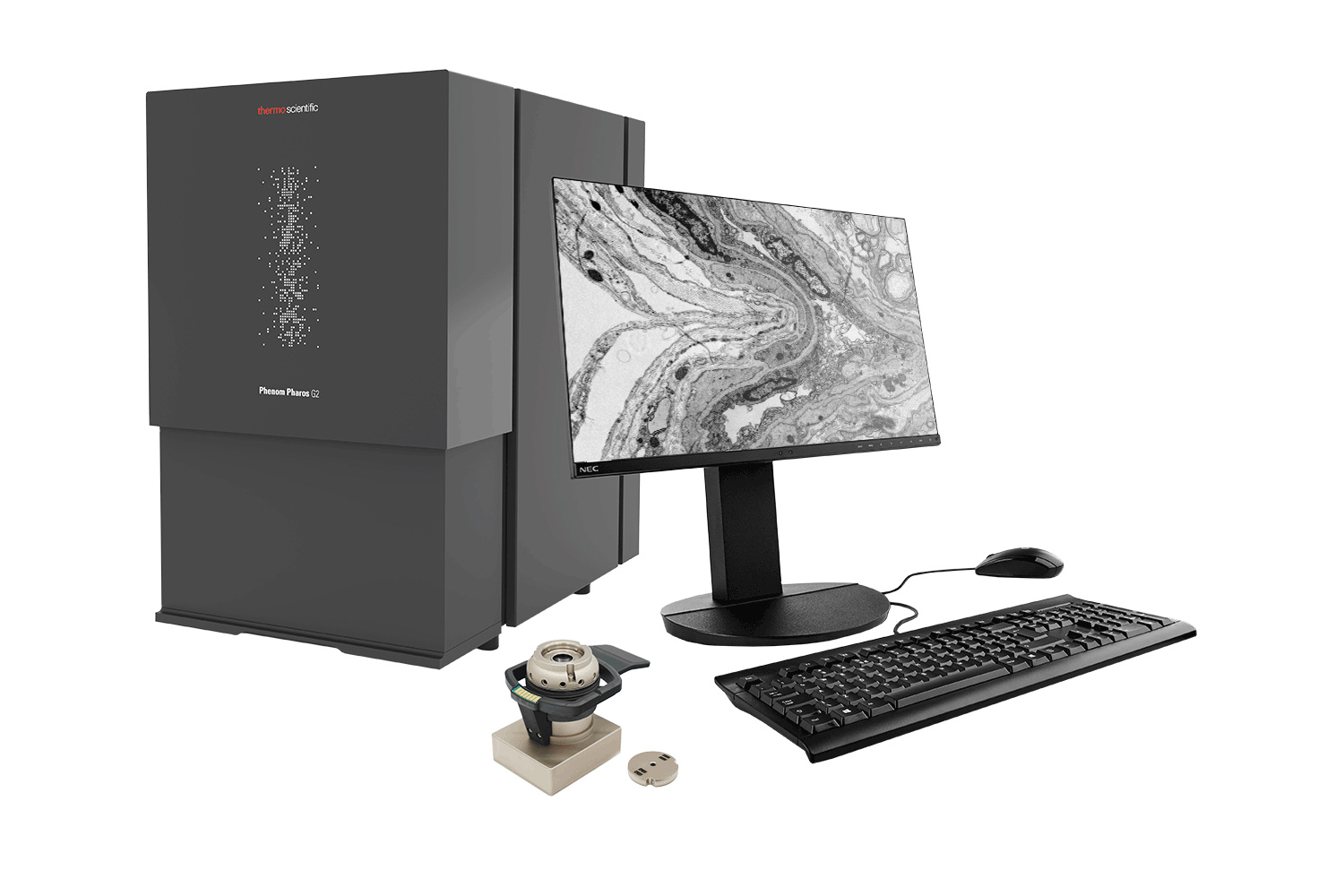
The Phenom Pharos STEM offers several advantages in both performance and usability. It provides high-contrast transmission imaging at low accelerating voltages, making it particularly suitable for beam-sensitive or biological samples, and supports large-area imaging (up to ~1.8 × 1.1 mm), significantly larger than typical tabletop TEM fields of view. The desktop footprint, minimal infrastructure requirements, and rapid “sample-to-image” workflow enable deployment in standard lab environments without the complexity of traditional TEM systems. Additionally, seamless switching between SEM and STEM modes allows users to screen, locate, and then analyze samples within a single instrument, improving throughput and workflow efficiency.
Its primary uniqueness lies in democratizing STEM imaging: unlike conventional TEM/STEM systems that require specialized facilities and expertise, the Pharos platform delivers fast, accessible, low-voltage STEM imaging with simplified operation and minimal training, while still providing multimodal capability (SEM + STEM + EDS). As a result, it serves as a cost-effective and high-throughput alternative for nanoscale characterization, particularly for applications such as nanoparticle analysis, biological screening, and routine materials characterization where atomic resolution is not strictly required.
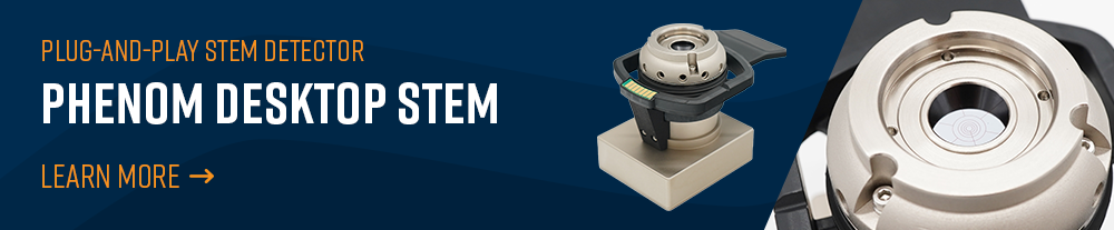
True STEM Detector in the Phenom Pharos:
The STEM capability in the Phenom Pharos Desktop SEM is enabled by a fully integrated, segmented transmission detector embedded directly within the STEM sample holder, as shown in Figure 4. This approach differs fundamentally from conventional Transmission Electron Microscopy (TEM)-based STEM systems, where detectors are fixed within the column and require more complex alignment and setup.
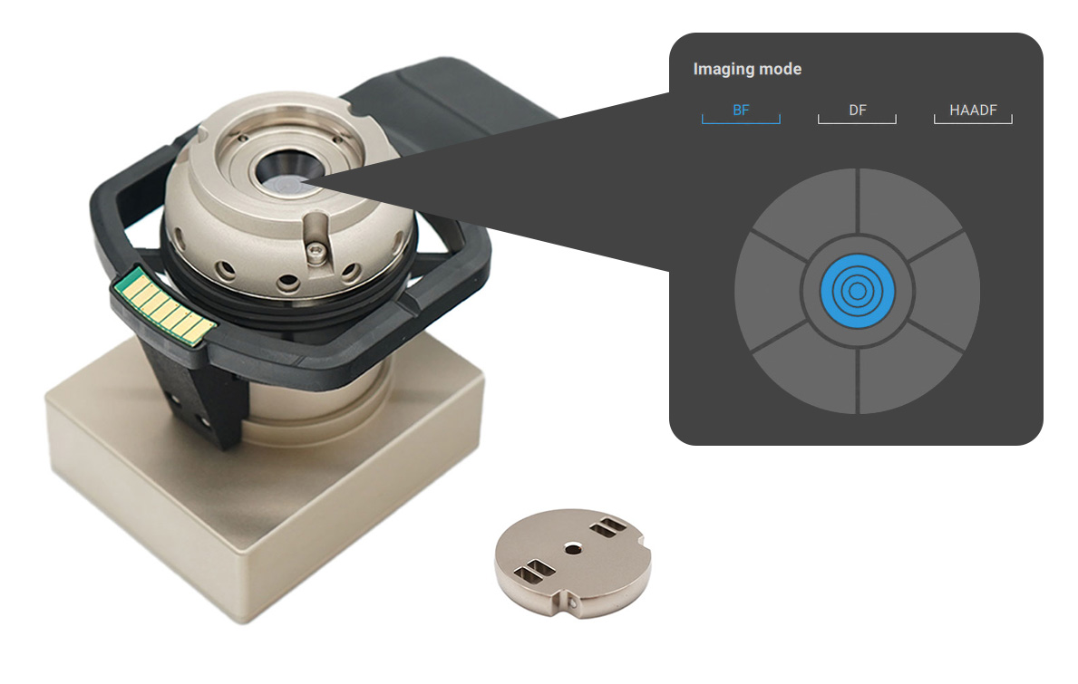
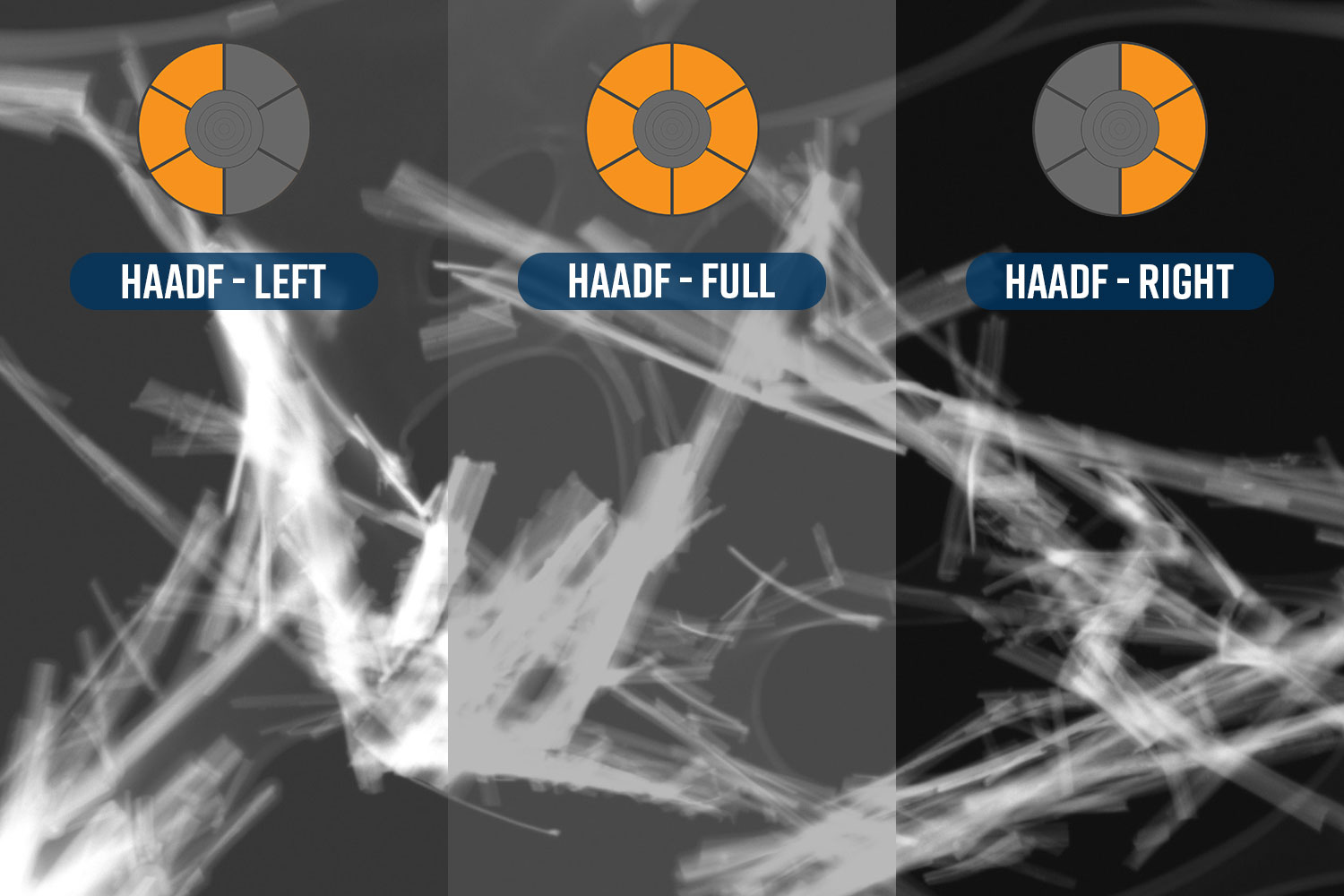
The Phenom STEM detector comprises multiple independently addressable segments, each corresponding to a defined electron scattering angle range. By selecting or combining these segments, users can configure imaging modes such as Bright Field (BF), Dark Field (DF), High-Angle Annular Dark Field (HAADF) (shown in Figure 5), or application-specific custom modes (Figure 6). Because the detector electronics are fully integrated into the holder, operation is inherently plug-and-play. Switching from SEM to STEM simply involves inserting the STEM holder.
The STEM detector is optimized for low accelerating voltages (typically 1 – 20 kV), maintaining strong signal levels even at reduced beam energies. This makes it particularly well suited for beam-sensitive materials such as tissue specimens, polymers, and other soft matter.
The detector design offers several practical advantages. It eliminates the need for manual alignment and is pre-optimized for standard imaging conditions with a fixed working distance, enabling straightforward operation even for non-specialist users. The workflow is highly efficient, with time-to-image typically under one minute, and the system is compatible with standard 3 mm TEM grids, simplifying sample handling and preparation.
Although originally developed for the Pharos platform, the STEM detector is also compatible with the Phenom Pro and ProX systems, extending access to transmission imaging capabilities across a broader installed base. This compatibility allows laboratories to incorporate STEM workflows without investing in a dedicated, high-cost TEM system.
While peak resolution performance is achieved on the Pharos system, the detector delivers a substantial enhancement in imaging capability on Pro and ProX platforms. It still enables improved structural visualization and access to internal features that are not attainable using conventional SEM imaging alone.
Conclusion
STEM is a high-resolution, information-rich technique that provides transmission-based insight into the internal structure and composition of materials, making it indispensable for advanced materials research and nanoscale characterization. In practice, STEM and SEM are complementary: SEM is typically used for rapid surface screening and localization, while STEM is applied for high-resolution, in-depth analysis of internal structures and targeted regions.
The Phenom Pharos STEM is a hybrid SEM–STEM platform that integrates transmission imaging into a compact, user-friendly desktop system. Its STEM capability is enabled by a segmented transmission detector embedded within the sample holder, engineered for simplicity and operational flexibility. By selectively collecting electrons over defined scattering angles, the Phenom STEM detector supports Bright Field (BF), Dark Field (DF), High-Angle Annular Dark Field (HAADF), and customizable imaging modes, while achieving sub-nanometer resolution at low accelerating voltages. This architecture emphasizes ease of use, rapid workflow, and adaptable contrast mechanisms, effectively extending STEM imaging to environments beyond traditional high-end electron microscopy facilities.
References
- Pennycook, S. J.; Li, C.; Li, M.; Tang, C.; Okunishi, E.; Varela, M.; Kim, Y.-M.; Jang, J. H. Material structure, properties, and dynamics through scanning transmission electron microscopy. Journal of Analytical Science & Technology 2018, 9 (1), 11. https://doi.org/10.1186/s40543-018-0142-4 ↩︎