Ceramics often have grain sizes and microstructure that impact material performance. Scanning electron microscope (SEM) images are used to quantify the grain sizes and distribution. Grain boundaries and microstructure can be optimized with ceramic processing parameters for specific product requirements.
Ceramic Grain Size and Coverage
Backscattered electron detector (BSD) images, like the advanced ceramic heating element material below, inherently provide material contrast. This allows for easy threshold and analysis of SEM images for ceramic materials to determine grain size and area.
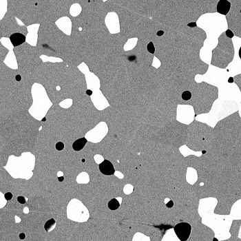
Many ceramic materials are sintered to produce the required mechanical properties. Grain size and coverage can be quantified using BSD SEM images. Using Automated Image Mapping with the Phenom SEM, data acquisition can be automated for maximum workflow with statistical analysis.
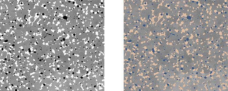
This is illustrated with a tiled image comprised of 30 individual SEM image (below left). Total acquisition time is under 3 minutes. The tiled image is then analyzed using a threshold effect, shown below on the right, indicating 5% black, 78% gray, and 17% white for this ceramic sample. The grain distribution data can be used to optimize processing conditions to meet product requirements.