Tech Note | Technology: Ion Milling, Scanning Electron Microscopy
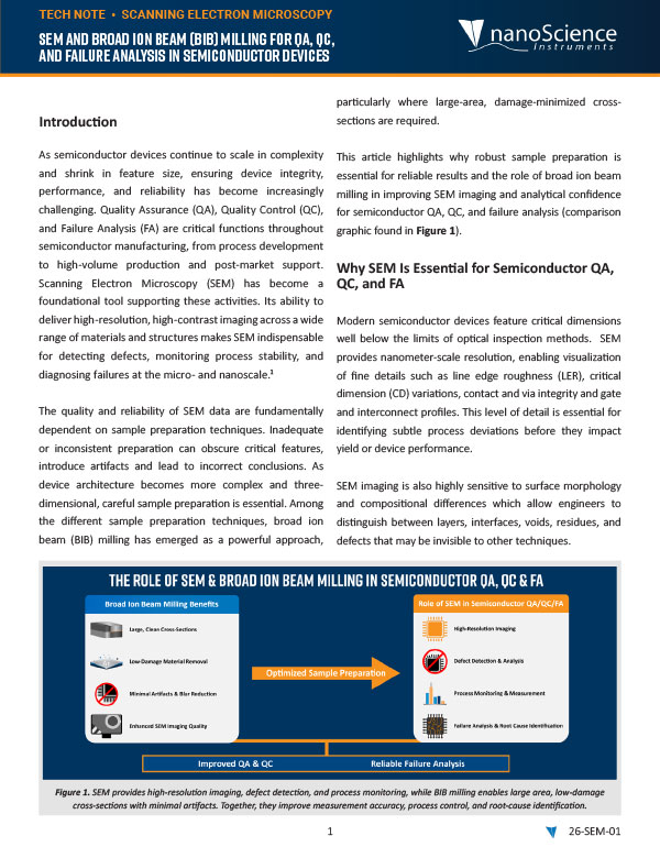
Introduction As semiconductor devices continue to scale in complexity and shrink in feature size, ensuring device integrity, performance, and reliability has become increasingly challenging. Quality Assurance (QA), Quality Control (QC),…
Tech Note | Technology: Scanning Electron Microscopy
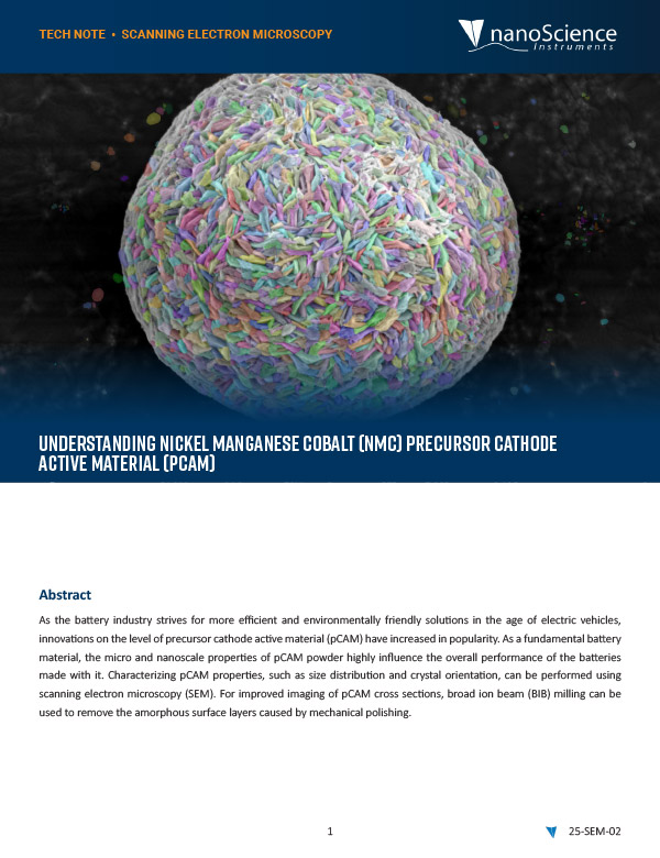
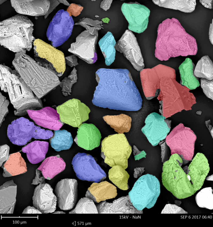
As the battery industry strives for more efficient and environmentally friendly solutions in the age of electric vehicles, innovations on the level of precursor cathode active material (pCAM) have increased…

Tech Note | Technology: Scanning Electron Microscopy
In today’s precision-driven manufacturing landscape, part cleanliness isn’t just a quality benchmark, it’s a critical factor that can make or break product performance and reliability. This is especially relevant in…
Tech Note | Technology: Scanning Electron Microscopy
The Phenom Pharos Desktop SEM/STEM is a compact and affordable solution designed for cryo-electron microscopy groups and core facilities looking to streamline experimental workflows. This technical note evaluates the Phenom…

Tech Note | Technology: Scanning Electron Microscopy
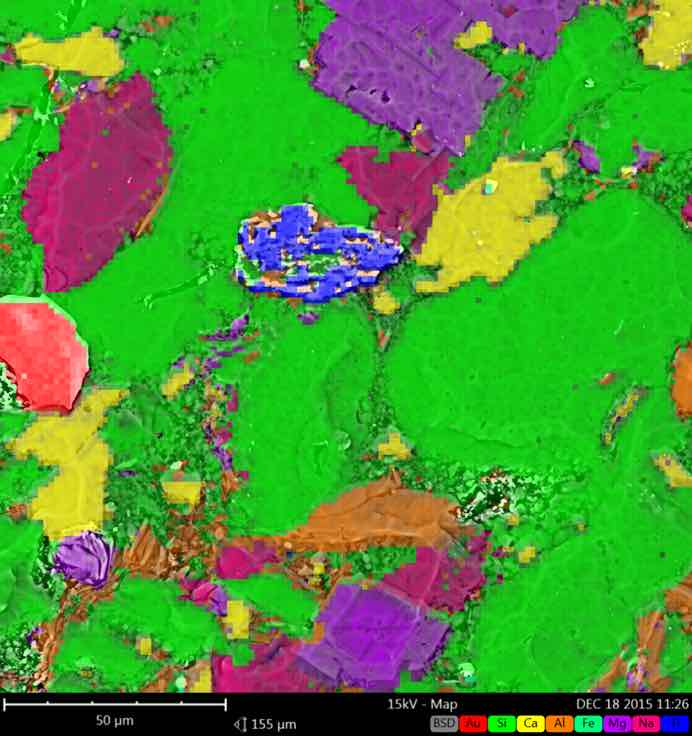
In modern steel manufacturing, non-metallic inclusions represent a critical quality concern due to their effects on mechanical properties and overall steel functionality. Scanning electron microscopy (SEM) and energy dispersive X-ray…
Tech Note | Technology: Ion Milling
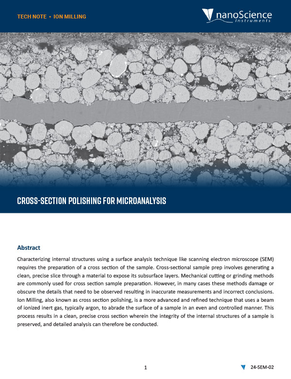
Characterizing internal structures using a surface analysis technique like scanning electron microscope (SEM) requires the preparation of a cross section of the sample. Cross-sectional sample prep involves generating a clean,…
Tech Note | Technology: Scanning Electron Microscopy
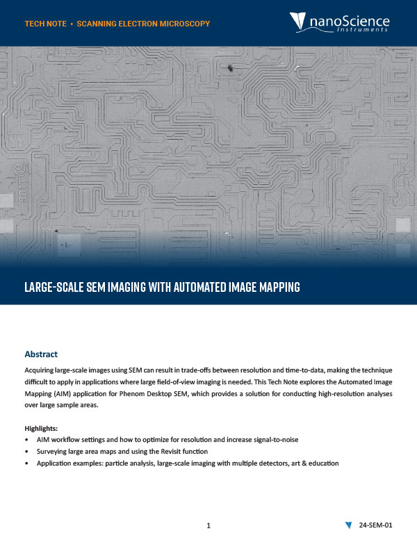
Acquiring large-scale images using SEM can result in trade-offs between resolution and time-to-data, making the technique difficult to apply in applications where large field-of-view imaging is needed. This Tech Note…
Tech Note | Technology: Scanning Electron Microscopy
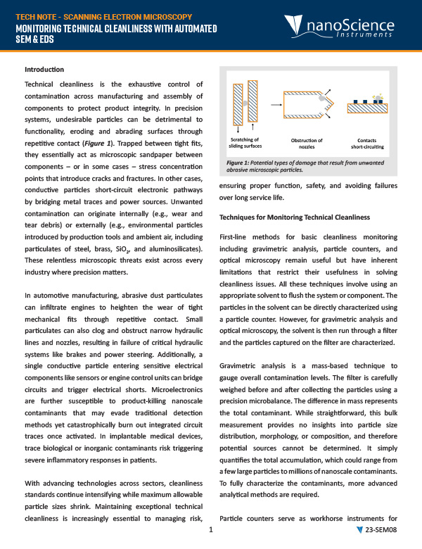
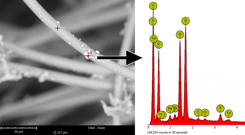
Technical cleanliness is the exhaustive control of contamination across manufacturing and assembly of components to protect product integrity. In precision systems, undesirable particles can be detrimental to functionality, eroding and…
Tech Note | Technology: Scanning Electron Microscopy
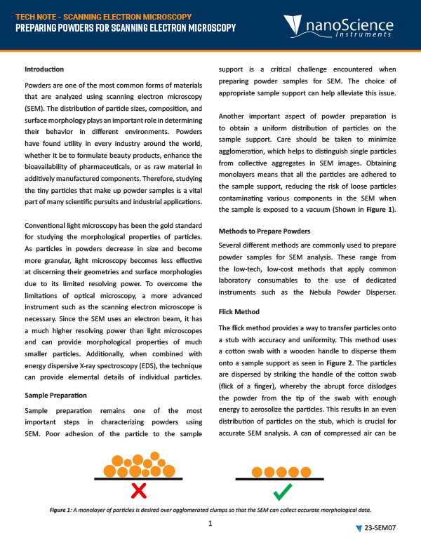
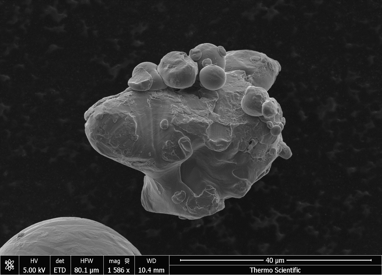
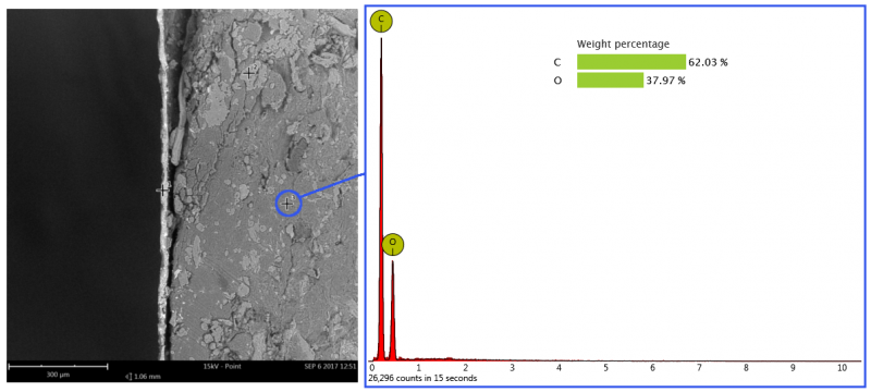
Powders are one of the most common forms of materials that are analyzed using scanning electron microscopy (SEM). The distribution of particle sizes, composition, and surface morphology plays an important…

App Note | Technology: Scanning Electron Microscopy
Fuel cells are electrochemical devices that can provide clean, renewable energy for widespread applications, from powering handheld devices to entire buildings. Of the various fuel cell types, arguably the most…
Tech Note | Technology: Scanning Electron Microscopy
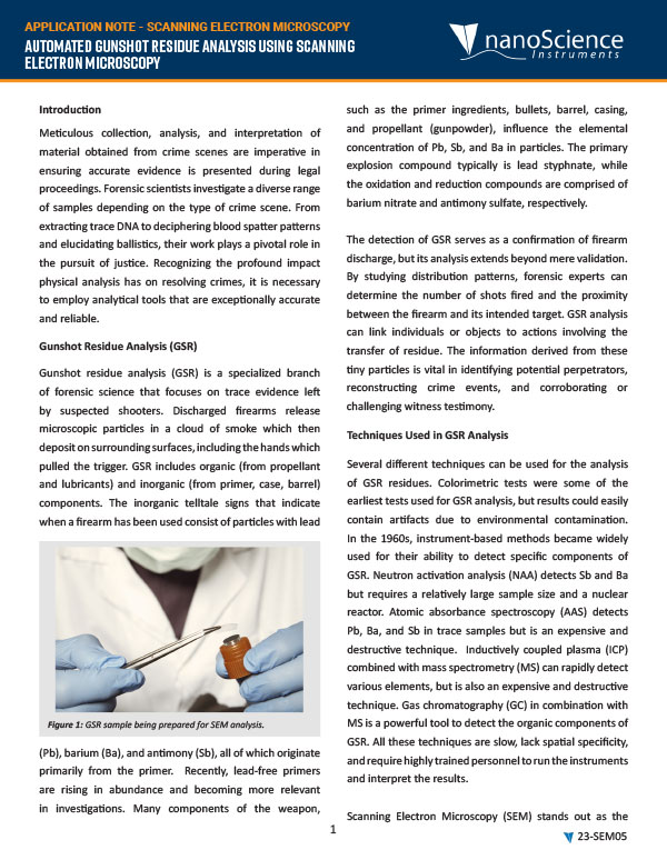
Meticulous collection, analysis, and interpretation of material obtained from crime scenes are imperative in ensuring accurate evidence is presented during legal proceedings. Forensic scientists investigate a diverse range of samples…
Tech Note | Technology: Scanning Electron Microscopy
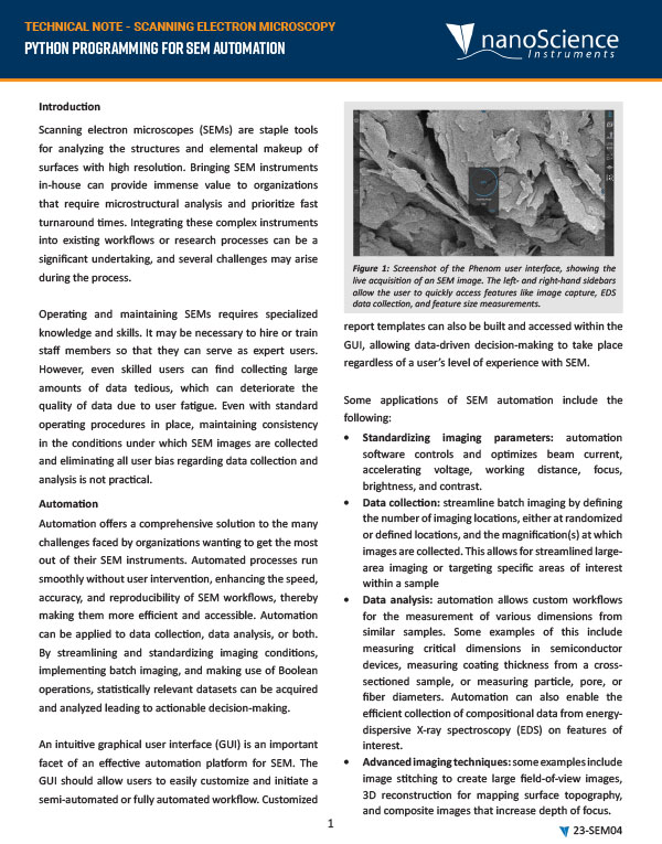
Scanning electron microscopes (SEMs) are staple tools for analyzing the structures and elemental makeup of surfaces with high resolution. Bringing SEM instruments in-house can provide immense value to organizations that…
App Note | Technology: Scanning Electron Microscopy
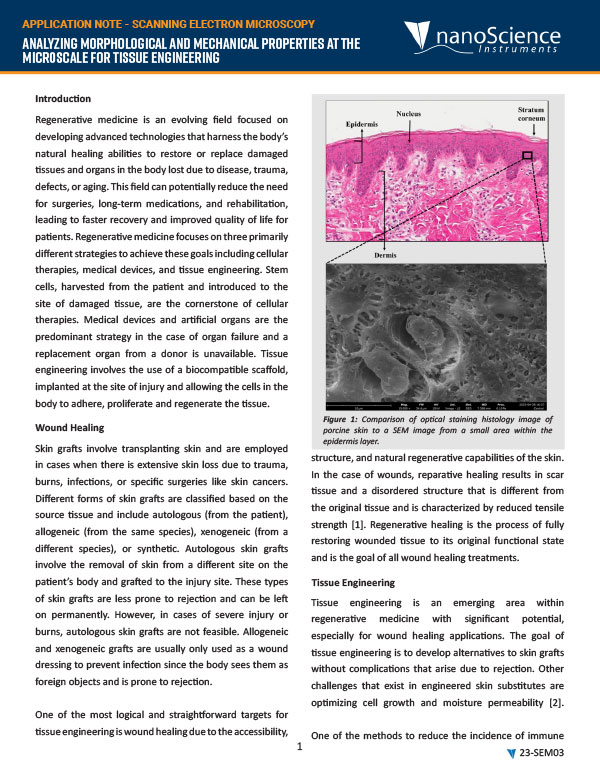
Regenerative medicine is an evolving field focused on developing advanced technologies that harness the body’s natural healing abilities to restore or replace damaged tissues and organs in the body lost…
App Note | Technology: Scanning Electron Microscopy
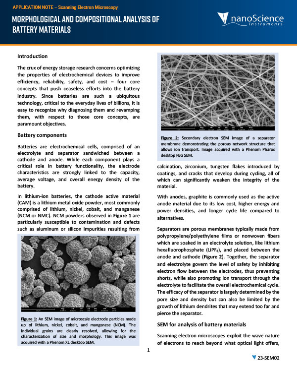
The crux of energy storage research concerns optimizing the properties of electrochemical devices to improve efficiency, reliability, safety, and cost – four core concepts that push ceaseless efforts into the…
App Note | Technology: Scanning Electron Microscopy
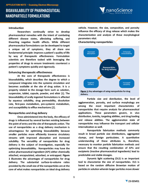
Every affliction of the body has its respective remedy, some targeted solution designed to alleviate or prevent negative health effects. Such remedies may have a long list of responsibilities to…
App Note | Technology: Scanning Electron Microscopy
In the past two decades additive manufacturing (AM) has rapidly evolved from a cutting-edge technology into a routine manufacturing method. The ability to quickly print complex shapes in a cost-effective…

App Note | Technology: Scanning Electron Microscopy
The rapid worldwide spread of the novel coronavirus, also known as COVID-19, has upended all conventional thinking regarding the scope of the damage it is causing and ways to control…

App Note | Technology: Scanning Electron Microscopy
The worldwide spread of COVID-19 has everyone questioning how to protect themselves and help those on the front line of the coronavirus. The CDC recommends facemasks be used for those…
App Note | Technology: Ion Milling
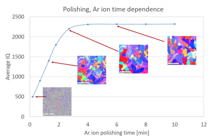
High Resolution Electron Back Scatter Diffraction (EBSD) and Scanning Electron Microscope (SEM) Surface/Cross Section Sample Preparation In Electron Back Scatter Diffraction (EBSD) studies, surface quality is a key issue. Diffraction…
App Note | Technology: Ion Milling
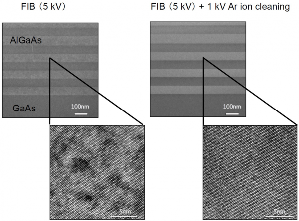
Focused Ion Beam (FIB) Sample Milling for High Performance Transmission Electron Microscopy Investigation (TEM) The use of focused ion beam (FIB) systems has become the method of choice for site-specific…
App Note | Technology: Scanning Electron Microscopy
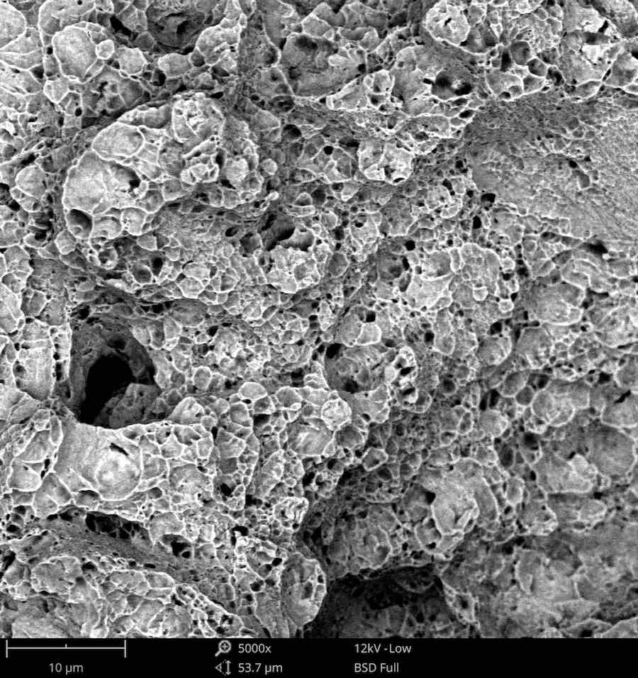
Fractography is a method in failure analysis for studying the fracture surface of materials. Studying the characteristics of the fractured surface can help to determine the cause of failure in…
App Note | Technology: Scanning Electron Microscopy
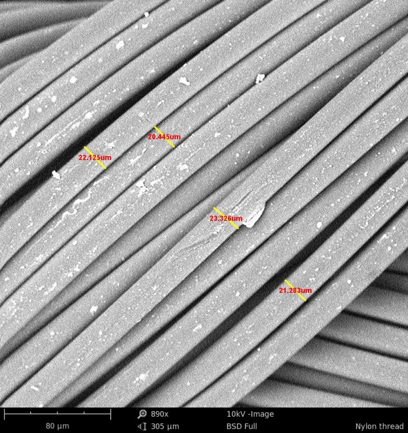
Fiber-based filtration systems clean everything from the air we breathe to the oil that runs our engines. Many filters, like high-efficiency particulate air (HEPA) and ultra-low particulate air (ULPA) filters,…
App Note | Technology: Scanning Electron Microscopy
Filtration and fibers used to separate liquids from particles or particles from air play an important role in our everyday lives. Filters help to clean air, water or oil for…
App Note | Technology: Scanning Electron Microscopy
Ceramics often have grain sizes and microstructure that impact material performance. Scanning electron microscope (SEM) images are used to quantify the grain sizes and distribution. Grain boundaries and microstructure can be…
App Note | Technology: Scanning Electron Microscopy
Scanning Electron Microscope Additional Signals Scanning electron microscopy is now a routine technology employed in the study of rocks and minerals. In addition to providing high-resolution images, electron microscopes generate a…
App Note | Technology: Scanning Electron Microscopy
Particle Analysis and characterization with the Scanning Electron Microscope (SEM) Understanding the physical characteristics of particles in dry powder materials is an essential aspect of drug product development. The particle…
App Note | Technology: Scanning Electron Microscopy
The Analytical Tools Needed for Deformulation of Pharmaceutical Imaging plays an integral role in the deformulation of any product. Separation and quantification of individual ingredients often require a suite of…