Scanning electron microscopy (SEM) grants access to the micro and nanoscale surface structure of materials, revealing their topography and elemental distributions. Manually surveying large areas on the order of several millimeters at high resolution via SEM can be a tedious, time-consuming process due to the inherently narrow field of view when working at high magnifications. SEM operators must choose whether to sacrifice resolution or time if examining such large areas is required.
To maintain resolution, a microscopist often opts to manually collect several high-magnification images systematically across the region of interest. The imaging parameters may need to be optimized in each sub-region which can take up considerable time. An encompassing view of the full area is achieved by manually stitching all images together to form a composite large-area map. On the other hand, the microscopist chooses to sacrifice resolution, and a single low-magnification image is acquired to encompass the full region of interest. The resulting resolution may be insufficient to make accurate measurements or observe key topographical features.
Automated solutions that enable rapid SEM data collection across large areas without compromising resolution offer several benefits across research and industrial applications, from reducing the risk of oversight in identifying critical features to making comprehensive sample analysis more efficient and accessible.
Phenom’s Automated Image Mapping
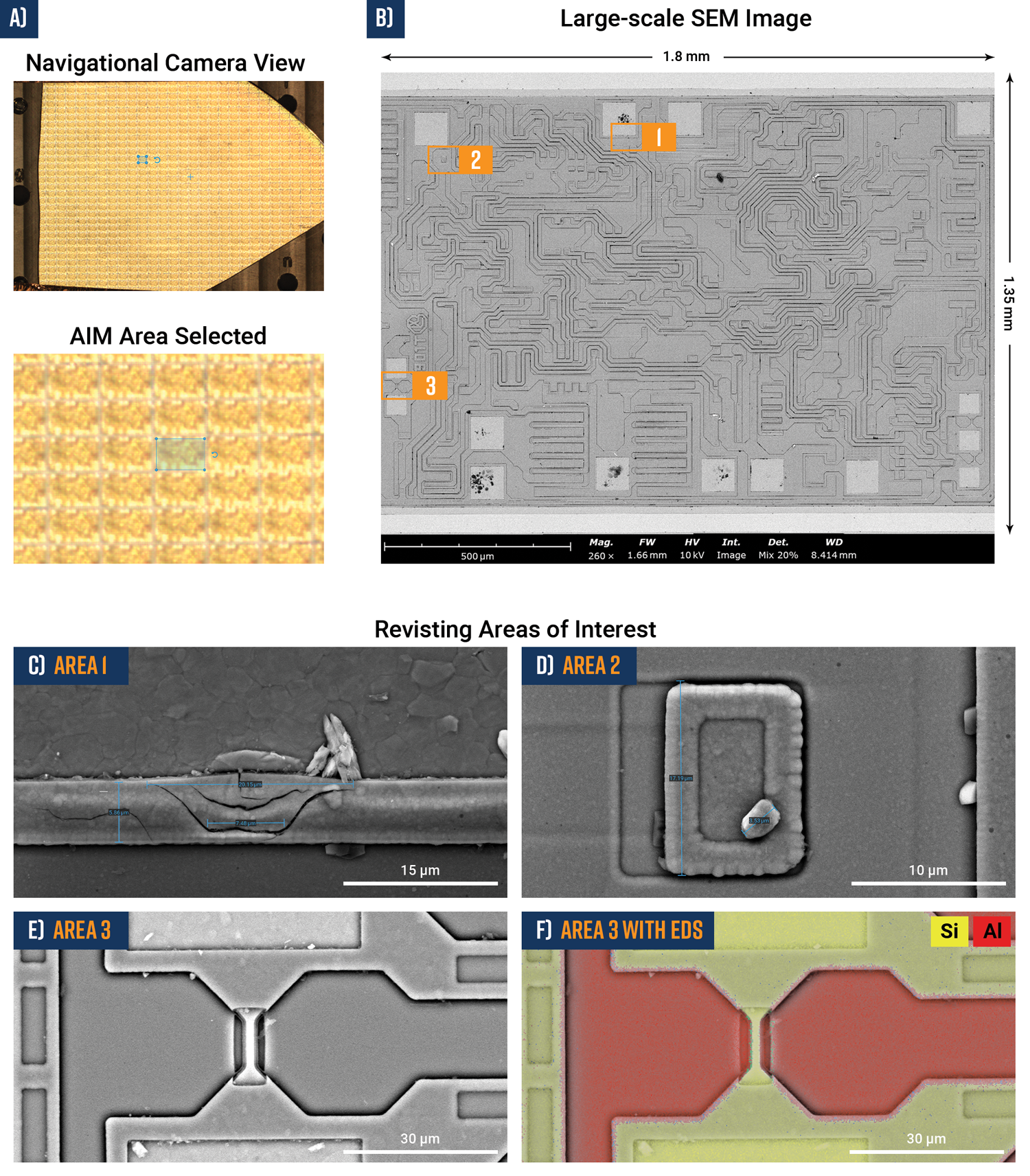
Automated Image Mapping (AIM) is a standard capability of all Phenom Desktop SEM models and allows the user to obtain large-scale SEM images at high resolution. This application solves the problems associated with manual acquisition by rapidly acquiring a set number of images across a predefined area and accurately stitching them into a seamless and in-focus large-area map. In addition, Auto Focus can be enabled to ensure images of sample areas with different depths are optimized. Figure 1a-b shows an example of a large-scale image acquired with a Phenom XL Desktop SEM of a silicon wafer patterned with integrated circuit (IC) dies. The full area encompasses 1.8 mm x 1.35 mm and is made up of 12 (4 x 3 array) individual SEM images. Each image is 450 µm x 450 µm and was acquired at a pixel size of 439 nm.
Figure 1. Automated Image Mapping of IC wafer: (a) Navigation Camera view of the sample, showing region selection for AIM and an enlarged view for detail. (b) Largescale SEM image acquired via Phenom’s AIM application, showing three areas selected for further analysis. Revisiting areas of interest: (c) Area 1 was used for crack dimension measurements, (d) Area 2 shows dimensional measurements of patterned feature and foreign particle; Area 3 contains another patterned feature which was used for further (e) imaging and (f) EDS mapping.
Revisiting Areas of Interest
When surveying a large-area map, the user can zoom in and pan the stitched image to scan for areas of interest. Right-clicking on any location will prompt the user with two choices: (1) export the current view of the map as either a .tiff, .jpeg, or .png, or (2) use the Revisit feature. By selecting Revisit, the stage will automatically drive to the same location and enter live SEM imaging mode.
Revisiting different areas of interest from a large-area map can be achieved by iteratively going back and forth from live SEM imaging to the recorded map as many times as needed, as shown in Figure 1c-e. Users can conduct further analysis at the site of interest by collecting a more detailed image at higher magnification, switching detectors, or acquiring an EDS map. Figure 1f shows an EDS map of area 3 which reveals the patterned features on the silicon wafer are predominately aluminum.
AIM Workflow
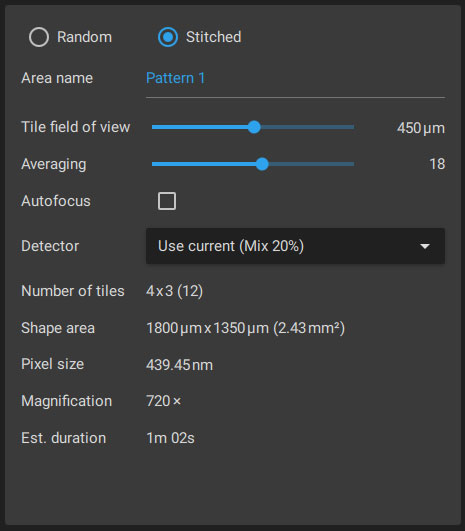
The first step in the AIM workflow is defining the region of interest. Defining a zone is as simple as clicking and dragging a rectangle on the optical image of the sample (Figure 1a). The software correlates each position selected through the Navigation Camera view to a position on the sample stage. The calculated area is displayed on the AIM settings panel in real-time. A screenshot of the AIM settings panel is shown in Figure 2, revealing the settings used to acquire the large-scale SEM image of the silicon wafer in Figure 1. The tile field of view – equivalent to a single SEM image – can be adjusted over a range of values using a slider bar or by entering a specific value. Changing the field of view parameter determines the magnification and corresponding pixel size, which are displayed toward the bottom of the panel. The user can use this information to optimize the resolution required for their application. The averaging value defines how many times each area will be scanned to acquire a single image. Increasing the number of scans improves signal-to-noise but also increases the total acquisition time.
The active electron detector setting in the AIM settings panel shows the default detector setting to be used for collecting the images. Phenom Desktop SEMs offer backscattered detector (BSD), secondary electron detector (SED), and a mixed mode where the ratio of BSD and SED signals can be defined (e.g., 25% BSD, 75% SED). If the detector listed in this window needs to be changed, the users will have to go back to live SEM imaging and activate the desired detector. All parameters can be saved as a template and retrieved for future AIM projects. This is a convenient feature in cases involving repetitious analysis.
Figure 2. The Automated Image Mapping settings panel displays key parameters that can be adjusted for a large area scan and offers the choice to save or load templates.
Applications of AIM
Large-area maps can be leveraged for a range of different applications, depending on the user’s goals. For example, the morphology and topography of a large feature can be examined in its entirety while also using the Revisit feature to examine specific regions of interest. Another example is to collect a large-area map to conduct statistically significant particle analysis. Data analysis software such as ParticleMetric can be used to quantify the particle size and shape distributions in large-area maps. Large-scale SEM images are extensively utilized in educational environments to acquaint students with microscopy and spark their interest in scientific inquiry.
Particle Analysis
When studying the morphology and size distribution of particulate samples through SEM, analyzing a statistically significant sample size in a reasonable timeframe can be a challenge. Larger sample sizes allow for more confidence in summary statistics and outlier particles to be readily identified, leading to a more comprehensive understanding of bulk powder properties. AIM solves this problem by rapidly generating large-scale SEM images at high resolution to maximize the number of particles analyzed.
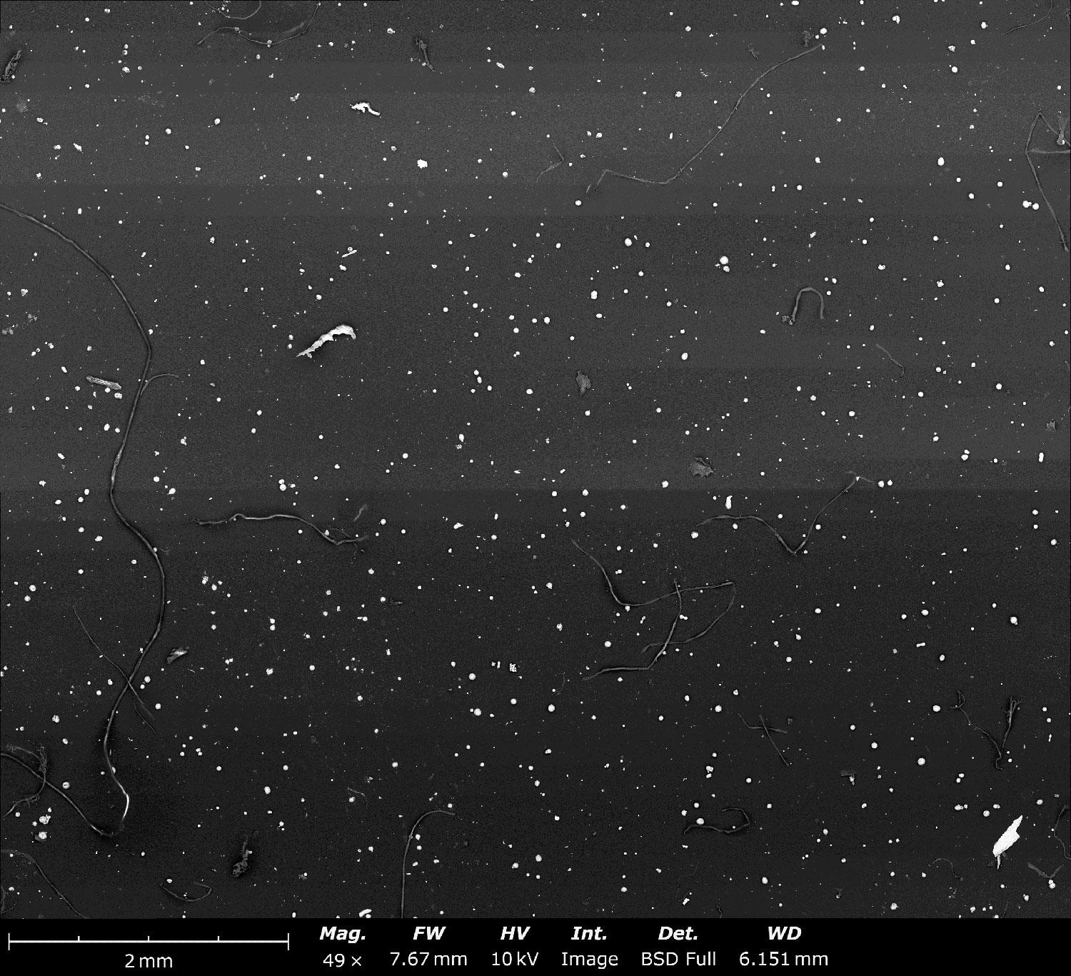
In the following example, a large-area map, covering 7.67 mm x 6.58 mm, is composed of 1050 individual images and captures 494 particles at high resolution (Figure 3). The large area map is then analyzed using ParticleMetric software, which automatically identifies and measures each particle based on an adjustable contrast threshold. Several metrics including size, circularity, diameter, and other geometric parameters for each particle can be rapidly analyzed and visualized.
Figure 3. Large-scale SEM image a sample showing 494 particles. Acquired with a Phenom XL Desktop SEM using AIM.
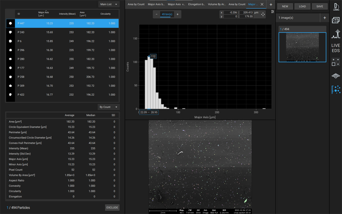
Figure 4 shows the ParticleMetric interface. Summary statistics, as well as individual measurements for circle equivalent diameter, area, perimeter, circularity, and other 11 parameters can be viewed on the left-hand panel of the interface. The data plotting panel can be used to visualize particle measurements through histograms or two-axis scatter plots.
Figure 4. The ParticleMetric software user interface shows all 15 geometrical quantities that are automatically calculated for each particle in the stitched map. Also visible are the colorized image map (bottom right), and the data plotting panel (top right).
Largescale SEM imaging with Multiple Detectors
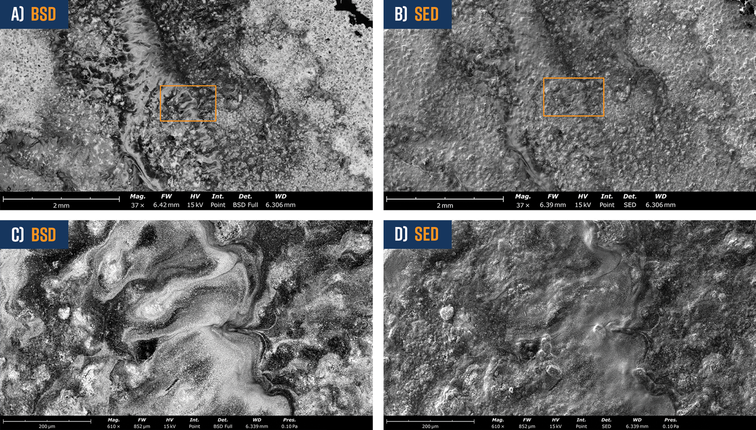
Correlative maps of large sample areas can be facilitated by applying the same AIM settings with two different detectors such as the BSD and SED. This type of approach can provide an initial broad overview of a sample surface which can help identify regions of interest to investigate further using the Revisit feature. Simultaneously, complementary information on surface composition and topography can be visualized side-by-side and explored at high resolution, which can help facilitate a more comprehensive understanding of how materials processing affects sample characteristics.
One example where correlative large-area mapping proves to be valuable is in analyzing catalyst distribution in polymeric exchange membrane (PEM) layers. The PEM layer is a critical component to the overall functioning of fuel cells as they control the flow of protons through the membrane electrode assembly. These are typically coated with a platinum catalyst layer which facilitates oxidation on the anode surface. Therefore, gaining an understanding of the platinum catalyst distribution on the PEM surface can help in optimizing fuel cell performance and durability.
Figure 5a-b shows large SEM images acquired with the BSD and SED detectors of a platinum-coated PEM surface over an area of 6.5 mm2. The BSD image contrast represents the elemental composition variations across the surface, where brighter contrast indicates higher densities of platinum. The contrast in the SED image is caused by surface topographical variations which can result from bumps, dimples, pores, and channels in the high-density polymer. High-resolution SEM images from individual sub-regions show a more detailed view from individual regions within the larger field of view (Figure 5c-d). By comparing both images side-by-side, a rough correlation between the catalyst distribution and surface topography can be observed.
Figure 5. Large area (a) BSD and (b) SED images of a catalyst-coated PEM surface acquired with the AIM function on a Phenom XL Desktop SEM. An individual SEM image from each sub-region is enlarged to show more detail from each imaging mode: (c) BSD and (d) SED.
Art & Education
In addition to enabling scientific analysis, the compelling images produced by AIM also open new avenues for artistic creativity and education, inviting the eye to explore detailed landscapes of the microscopic realms generated by hundreds of SEM tiles stitched together. Bridging science, technology, and creative expression together unveil the microscopic world in stunning detail – encouraging artists and students alike to explore the grandeur of nature on the smallest of scales.
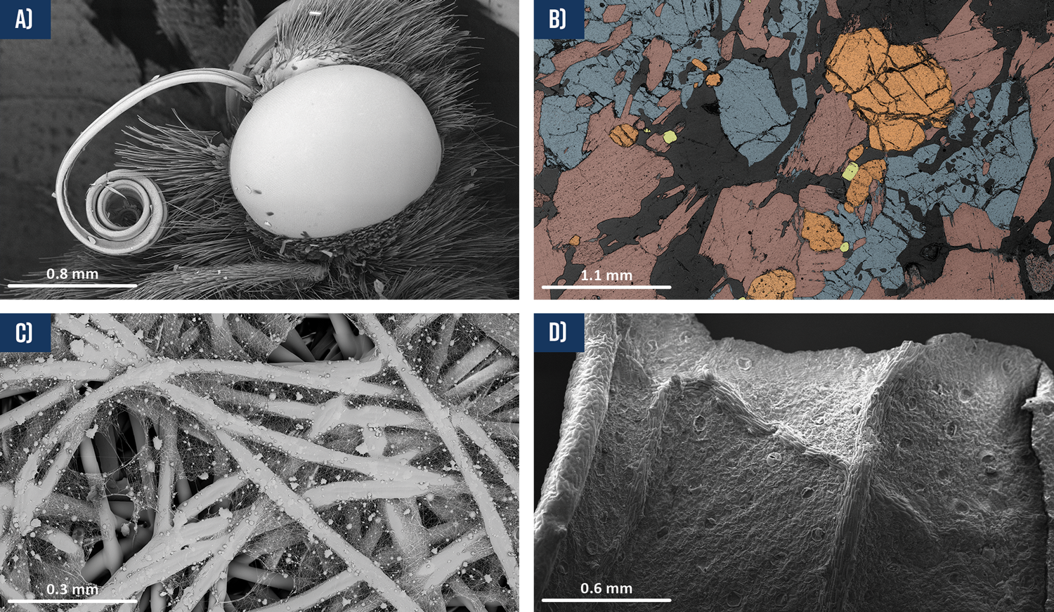
Figure 6 represents four examples of large-scale SEM imaging that demonstrate value in art and education. School programs that implement this type of information support students in developing an appreciation of the micro and nanoscales, and that appreciation in turn helps them understand how microstructures play a role in macroscale properties. Biology classrooms can benefit from high-resolution maps like the image of a butterfly (Figure 6a) during entomology investigations. Geology classrooms can identify the different elements that compose minerals such as the Gneiss metamorphic rock with EDS (Figure 6b). Microstructures of everyday materials, like fibers (Figure 6c) or peppermint (Figure 6d) observable with SEM can inspire further interest in science and technology or simply spur artistic creativity through nature’s designs.
Figure 6. A collection of various educational and artistic AIM projects: (a) butterfly face, (b) colorized Gneiss metamorphic rock, (c) electrospun filtration media, (d) peppermint particulate.
Summary
In summary, Phenom’s Automated Image Mapping technology enables efficient acquisition of high-resolution SEM images over large sample areas. By automatically stitching together arrays of image tiles, it produces seamless composite views spanning millimeters with details on the nanoscale. Researchers across disciplines can tremendously benefit from this multiscale perspective, visually accessing structures and textures within their larger surrounding contexts and conveniently revisiting areas for further analysis. Additionally, the software automation frees users from tedious manual microscopy, accelerating analysis through an advanced approach to wide-area nanoscale imaging.