Focused Ion Beam (FIB) Sample Milling for High Performance Transmission Electron Microscopy Investigation (TEM)
The use of focused ion beam (FIB) systems has become the method of choice for site-specific transmission electron microcscopy (TEM) sample preparation. Although focused ion beam offers advantages over conventional mechanical and chemical TEM sample preparation, it also has the drawback of high-energy operation. The high-energy Gallium (Ga+) ion beams used in focused ion beam systems form defected, amorphous and/or implanted layer in the specimen. FIB in general produces TEM samples which are less suitable for high performance analytical (S)TEM (HRTEM, HRSTEM, high spatial resolution EELS and EDX) investigations. However, for high-resolution microscopy and high-sensitivity analysis, low-energy Argon (Ar+) ion milling is ideal for the final stage of specimen preparation in order to decrease the defected layer.
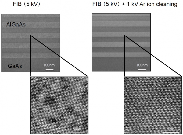
Technoorg’s Gentle Mill is ideal for cleaning and final polishing of FIB samples. With its low-angle, low energy broad Argon (Ar+) ion beam, it is suitable for removing the damaged layers created by the FIB during lamellae formation and also for further reducing the specimen thickness. The Gentle Mill is equipped with a dedicated, patented, low-energy ion gun down to 100eV ion energy which allows finishing of silicon FIB samples in about 10 minutes for each side.
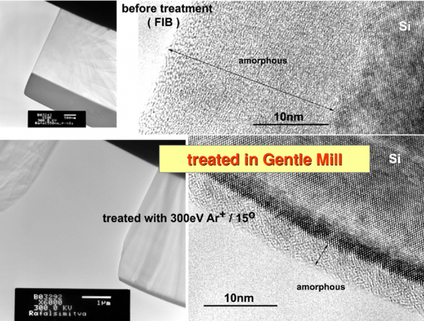
Preparation time can drastically be decreased when combining Hitachi’s FIB/STEM and Technoorg’s Gentle Mill systems. The Gentle Mill has been modified to allow the direct insertion of the FIB-STEM/TEM compatible specimen rotation holder. The Argon (Ar+) ion milling of FIB sample by Gentle Mill at 200eV reduces the amorphous layer in Si from 28nm to 1.2nm and reduces sample preparation time (FIB milling time: about 60 minutes, low-energy Ar+ ion milling time: 3 minutes), meeting the analysis requirements of high-throughput semiconductor devices.
1. T. Yaguchi et al.: A method for 3 dimensional structural and compositional imaging of nano-materials, Proceedings of Microsc Microanal 12 (Supp 2) 2006, 528-529
2. T. Yaguchi et al.: Development of sample preparation method for three-dimensional structural and elemental analyses of a specific site and its application, Proceedings of MRS Fall Meeting, Boston, USA, Nov. 26-30, 2006.
3. T. Yaguchi et al.: A site-specific structure analysis of a 65nm node device using a FIB-STEM/TEM system, Hitachi EM News, 2007, pp 25-30
4. T. Yaguchi et al.:A method for site-specific specimen preparation of Si device after 65nm node technology using FIB-STEM/TEM system, Proceedings of Microsc Microanal 13 (Supp 2) 2007, 790-791