Empowering Nanofibers: Enhancing Usability and Overcoming Production Challenges
Nanofibers, or fibers with diameters on the scale of 10-9 meters, exhibit unique properties, differing significantly from the properties of the bulk materials. These include a large surface area to volume ratio, high porosity, high encapsulation efficiency, superior mechanical properties, and higher chemical stability. As a result of these remarkable properties, some versatile materials have found their way into a multitude of applications with the potential to address critical challenges in numerous fields and lead to a more sustainable and technologically advanced future.
AVS 69th International Symposium | Nov. 7-9, 2023 | Portland, OR

AVS International Symposium and Exhibition Nanoscience Instruments is excited to announce our return to the AVS International Symposium in 2023! We will be showcasing the breadth of our surface science and electron microscopy solutions, including Quartz Crystal Microbalances with Dissipation monitoring (QCM-D), optical and force tensiometers, desktop Scanning Electron Microscopes (SEM), and SEM sample prep […]
7 Recent Advancements in Nanofiber Applications
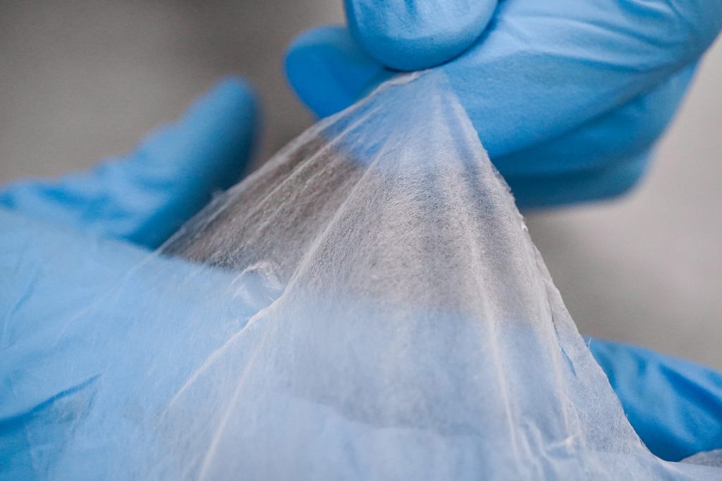
Nanofibers are ultrafine fibers with diameters typically ranging from a few nanometers (nm) to a few hundred nanometers. To put this in perspective, a nanometer is one billionth of a meter, and the width of a human hair is about 80,000 nm. Super small!
The Role of SEM in the Medical Device Industry

Implantable medical devices are continually pushing the boundaries of what is possible when modern medicine and engineering join forces. An implantable medical device is an instrument that is surgically inserted into a patient’s body to restore or enhance function to diseased or injured parts of the body. Common examples include pacemakers for correcting heart arrhythmia, […]
Particle Analysis in Additive Manufacturing
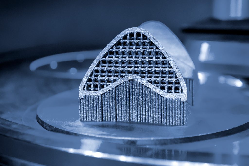
From supersonic jets to prosthetic knees, 3D-printed parts are revolutionizing design and production across industries. Printed components are no longer just prototypes, but now perform critical functions in the realms of aerospace, medical, dental, automotive, and beyond.
International Materials, Applications & Technologies 2023 | Oct. 16-19, 2023 | Detroit, MI
International Materials, Applications & Technologies 2023 Nanoscience Instruments cultivates global partnerships to deliver cutting-edge electron microscopy, surface analysis, and material characterization solutions. Visit our booth for a live, hands-on demonstration of an automated desktop Scanning Electron Microscope (SEM). In conjunction with the Attension line of tensiometers, these unique instruments enable transformative advancements in materials development […]
The Role of Scanning Electron Microscopy in the Automotive Industry

From zippy city scooters to heavy duty haulers, modern automobiles are assemblies of thousands of precisely manufactured components working in harmony to ensure smooth and safe rides. Beneath the sleek exteriors and plush interiors are components that at one point underwent stringent inspection for microscopic defects, particulates, and structures that could negatively impact performance, durability, […]
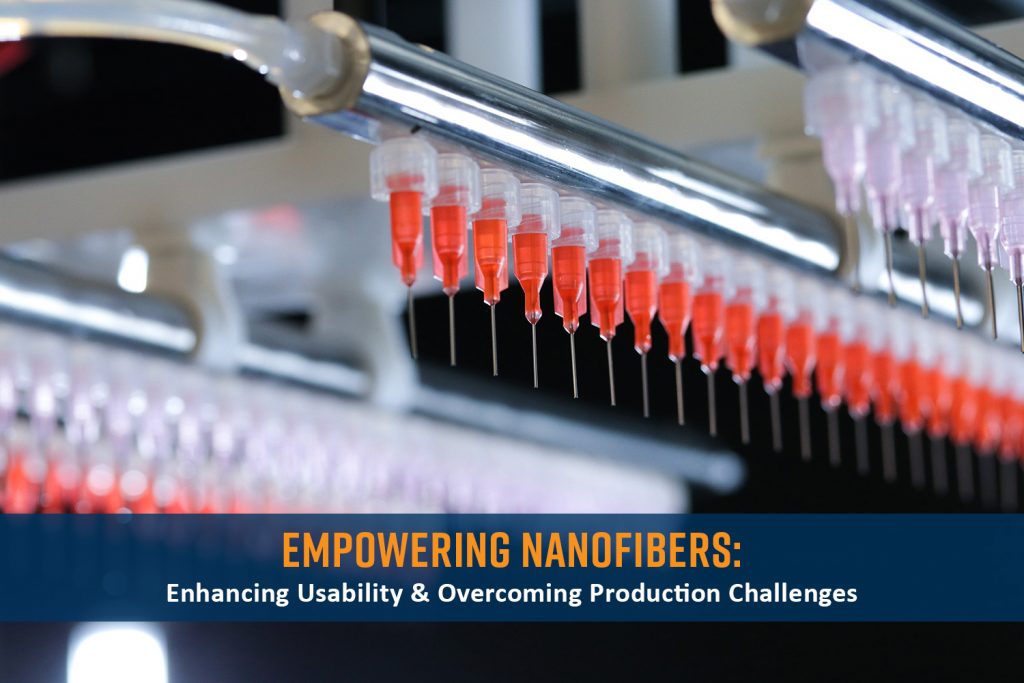
7 Factors to Consider While Buying an Electrospinning Machine

Electrospinning is a versatile nanofiber fabrication technique wherein a polymer solution is charged and ejected from a spinneret under a high-voltage electric field. As the polymer is ejected, the solvent evaporates, and a fine jet of polymer forms, which elongates and solidifies into nanofibers upon reaching an oppositely charged or grounded collector. The resulting nanofiber […]
Medical Device & Manufacturing Minneapolis 2023 | Oct. 10-11, 2023 | Minneapolis, MN

Nanoscience Instruments and our sister company, Nanoscience Analytical, provide cutting-edge instrumentation and process development services to enhance the production of medical devices and biomedical products such as tissue scaffolds, vascular grafts, wound healing therapeutics, and more.
Applications of SEM in Semiconductor Device Failure Analysis
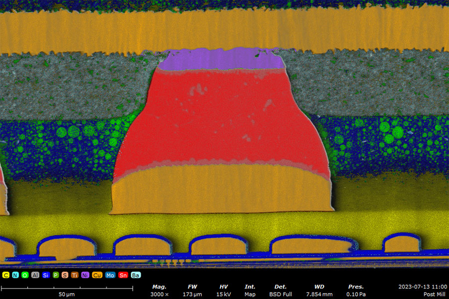
Failure analysis (FA) is an essential methodology that engineers use in the development process of semiconductor devices, like the CPU found in your smartphone or laptop. It involves the application of multiple analytical tools to isolate the root cause of a particular failure mode to prevent it from happening in the future. Failure modes describe how a device is failing by not meeting a certain electrical, mechanical, or visual specification.