Failure analysis (FA) is an essential methodology that engineers use in the development process of semiconductor devices, like the CPU found in your smartphone or laptop. It involves the application of multiple analytical tools to isolate the root cause of a particular failure mode to prevent it from happening in the future. Failure modes describe how a device is failing by not meeting a certain electrical, mechanical, or visual specification.
Failure modes can be identified during the manufacturing process when a component fails an inline quality control test by being measured as “out-of-spec”. If enough units are impacted, the manufacturing yield will be reduced, and FA will likely be performed to understand the causes and potential solutions. Another way in which failure modes can be identified is during reliability testing. In these cases, FA is used to diagnose the physical origin of electrical failures such as delamination, buried cracks, or other physical defects.
Why is SEM essential for semiconductor FA?
FA often comes down to a needle-in-a-haystack search for a microscopic crack, delamination, or other physical defect in the vicinity of an electrical failure. The device itself may need to be cross-sectioned to reveal internal structures of interest. A fundamental requirement of the analytical tools used in FA is the ability to clearly visualize the components near the location where an electrical failure was detected.
Light microscopy is limited in terms of its resolution (~200 nm) and magnification range since it relies on visible light. Comparatively, SEM resolution ranges from around 1-10 nm which overall improves the ability to visualize much smaller defects such as cracks or delamination. Also, unlike optical microscopy, SEM is capable of a larger depth of focus which means that more features will remain in focus in a single field of view. This makes it much easier to survey a given area, identify potential defects, and make accurate dimensional measurements.
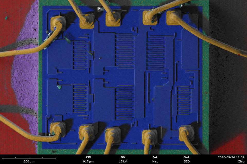
Scanning electron microscopy (SEM) is a standard tool used in FA not only because of its resolution and depth of field advantages but also because it can provide a comprehensive view of the sample using multiple detectors. The backscattered electron detector (BSD) and secondary electron detectors (SED) that are used to acquire images in the SEM provide complementary views of composition and surface topography, respectively. Another advantage of SEM is the ability to perform elemental analysis using an energy-dispersive X-ray (EDS) detector. EDS mapping is a great tool for detecting trace levels of contamination that can be correlated with structural characteristics.

What are some examples of how SEM can help with FA?
SEM is a powerful and versatile FA tool that is used for physical and compositional microanalysis. Some examples of how SEM is routinely used in semiconductor FA include:
Surface Inspection:
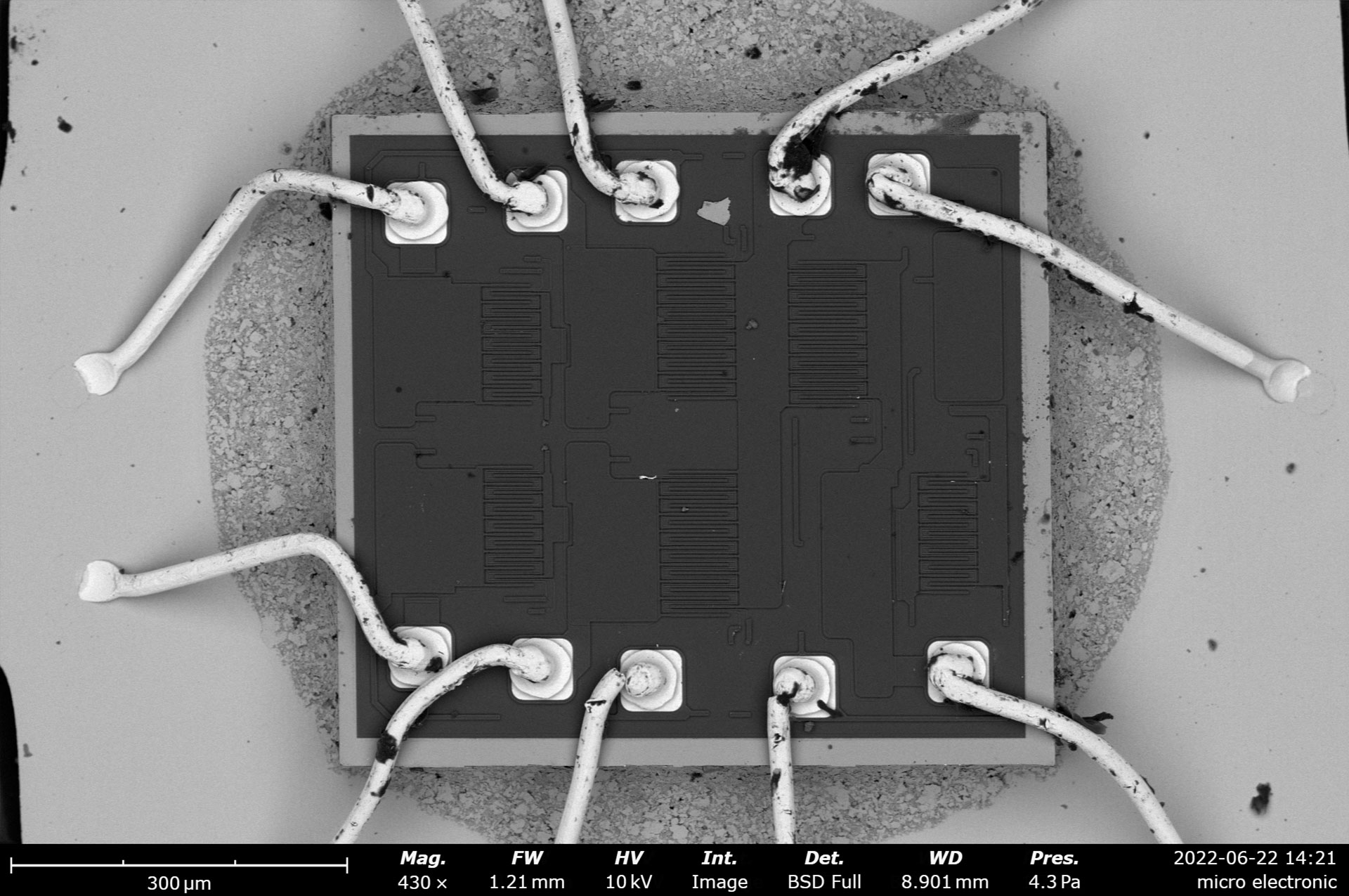
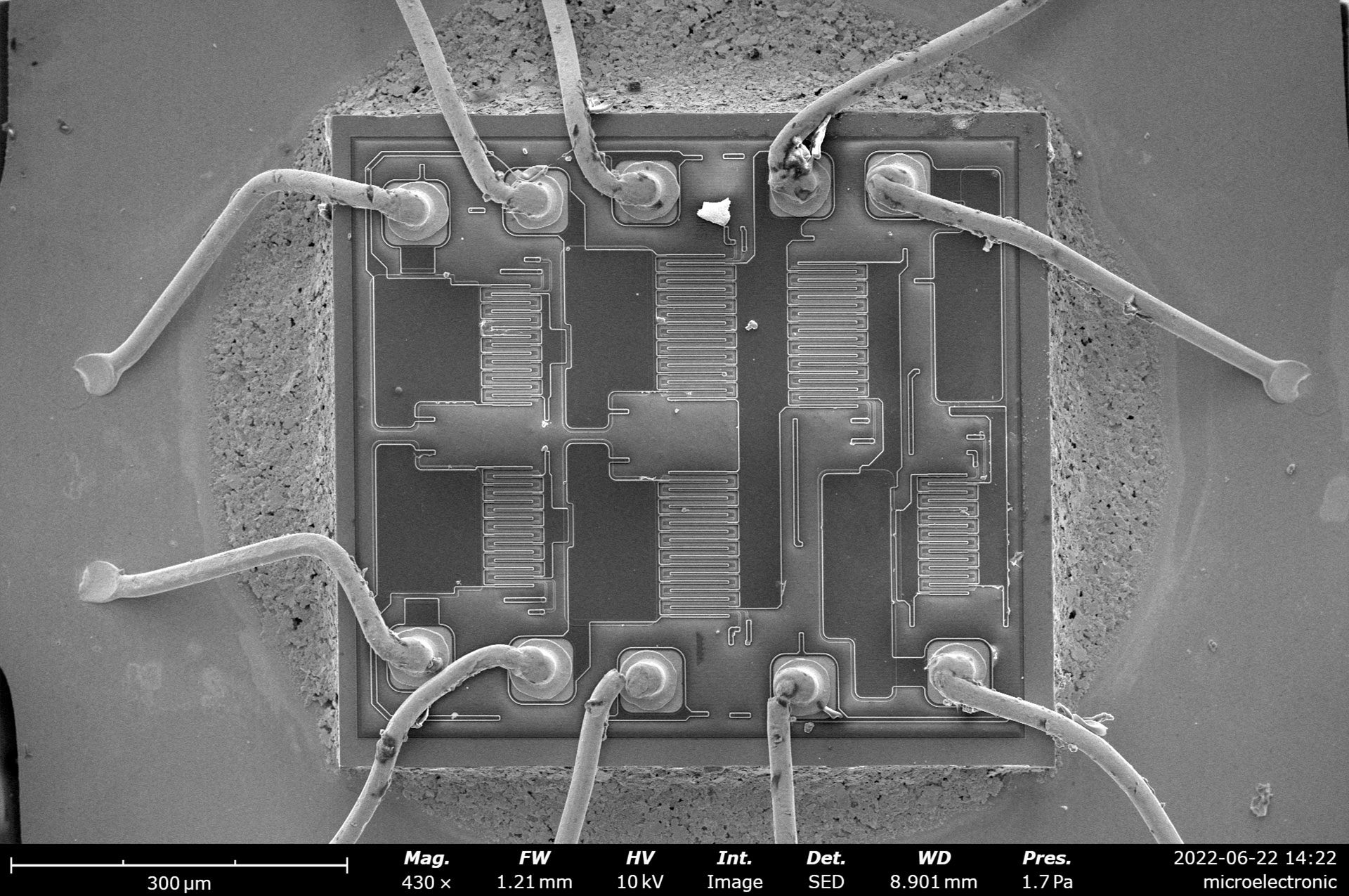
SEM can be used to identify failure modes including cracks, delamination, or contamination. Since the escape depth of secondary electrons is close to the surface (~2-5 nm in metals), the SED is useful for visualizing surface features. If the SEM has a segmented BSD, then qualitative topographic images can be generated by applying signal subtraction to the top/bottom or left/right halves. Topographic imaging mode can highlight features that may be more difficult to distinguish using the SED, allowing for acute identification of physical defects that impact device functionality. All Phenom Desktop SEM models come standard with a segmented BSD that contains four quadrants.
Elemental Analysis:
When combined with SEM imaging, EDS is highly valuable for semiconductor FA. EDS makes use of the X-rays emitted from the sample when it is irradiated with the scanned electron beam to identify the elemental composition of the sample. Using EDS analysis software, characteristic X-rays are identified, and the composition (in terms of atomic percentages or weight percentages) is calculated. By analyzing the elemental composition of the component materials, it is possible to identify impurities, alloy compositions, or any variation that may affect device performance or reliability.
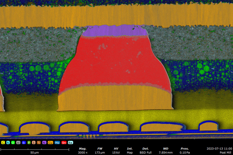
Imaging of cross-sections:
Semiconductor packages are often cross-sectioned at the suspected location of failure to reveal internal structures of interest. These samples are specifically prepared for SEM and EDS analysis. Some common examples of failures found via cross-sectioning are metallization issues, bridged bumps, interfacial delamination, voids in adhesives or underfill, and inconsistent metal plating.
Electron backscatter diffraction (EBSD):
EBSD is an SEM technique used to analyze the crystallographic orientation and microstructure of semiconductor and metallic materials. By mapping the crystal orientation and grain boundaries, EBSD can assist in identifying causes of corrosion or fracture in thin films, interconnects, and metal trace lines within semiconductor devices.
Particle analysis:
SEM can readily identify and analyze the size, shape, and composition of individual particles that may have caused shorting or mechanical damage to a device. Understanding the composition and other characteristics of foreign particles can help in identifying the root cause of contamination, whether it be from upstream processing, handling/storage media, or some other cause.
Electrical Characterization:
SEM can be combined with other techniques, such as focused ion beam (FIB) milling, to create electrical contacts on microscopic device features. The Phenom Desktop SEM is compatible with an Electrical Feedthrough Sample Holder, which has six quick-release pins that can be used to measure or apply voltages and currents to a sample during SEM imaging. These methods enable in-situ electrical testing and analysis of failed devices, providing insights into electrical failures such as opens, shorts, or leakage currents.
Summary
By utilizing these capabilities, SEM plays a crucial role in failure analysis within the semiconductor industry, assisting in the identification of failure mechanisms, improving device reliability, and guiding design and process improvements.