Scanning Electron Microscopy (SEM) is a powerful imaging technique used across various scientific and industrial fields to analyze surface morphology and structural composition at the nanoscale. Obtaining high-resolution images and performing accurate material characterization often requires specialized sample preparation techniques. Ion milling is one of the most effective techniques for this purpose and is widely used to thin, clean, and polish samples before SEM imaging. Ion milling ensures that artifacts from mechanical or chemical preparation do not interfere with imaging or elemental analysis, thereby enhancing clarity and accuracy. This article explores the fundamentals of ion milling, its working principles, and its diverse applications in electron microscopy, with specific real-world examples.
What Is Ion Milling?
Ion milling, also known as ion beam etching or ion polishing, is a physical etching technique that uses a beam of ions to selectively remove material from a sample’s surface. Ion beams are generated within ion sources and these ions are then accelerated onto a given sample. Material is physically sputtered away from the sample upon impact, and, with enough exposure, results in a polished surface. Heavier, inert elements, such as argon (Ar), are used as a source of ions in ion milling to maximize the sputtering efficiency while simultaneously avoiding any chemical alterations to the surface.
Types of ion milling can be generally separated into two categories, primarily characterized by the ion source being used and the diameter of the ion beam. Broad Ion Beam (BIB) milling generates a wide-area ion beam and commonly uses Ar ions to produce the ion beam. As the name implies, BIB is ideal for swift cleaning of sample surfaces and rapid, large area cross-section sample preparation. This technique benefits from the sheer scale of the achievable throughput while introducing minimal damage to the sample. A typical use case for BIB includes final surface polishing for electron backscatter diffraction (EBSD) to reveal the hidden grain structure of a sample.
Focused Ion Beam (FIB) milling, in contrast, uses a finely focused ion beam for site-specific material removal. FIB systems are typically housed within floor model SEMs, often referred to as dual beam SEMs or FIB-SEM. The level of precision operators can attain with these instruments is a massive benefit, even though they do take a lot of expertise and resources to operate. FIB is commonly used in semiconductor failure analysis and nanotechnology applications, as they can cut out small sections of material that house varying defects. Researchers need to choose the appropriate type of ion milling based on material properties and analytical requirements to optimize sample preparation.
Ion Milling in SEM
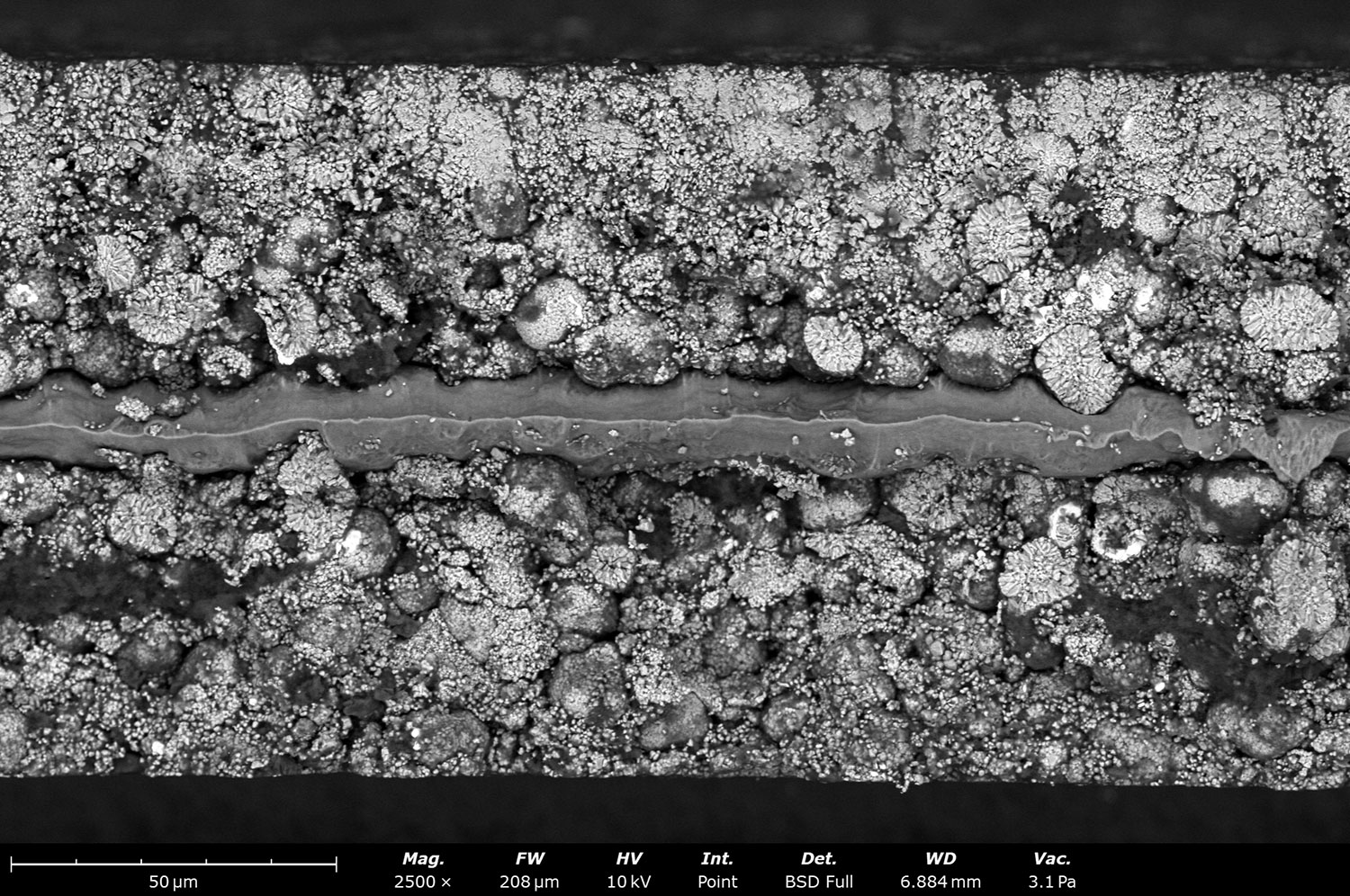
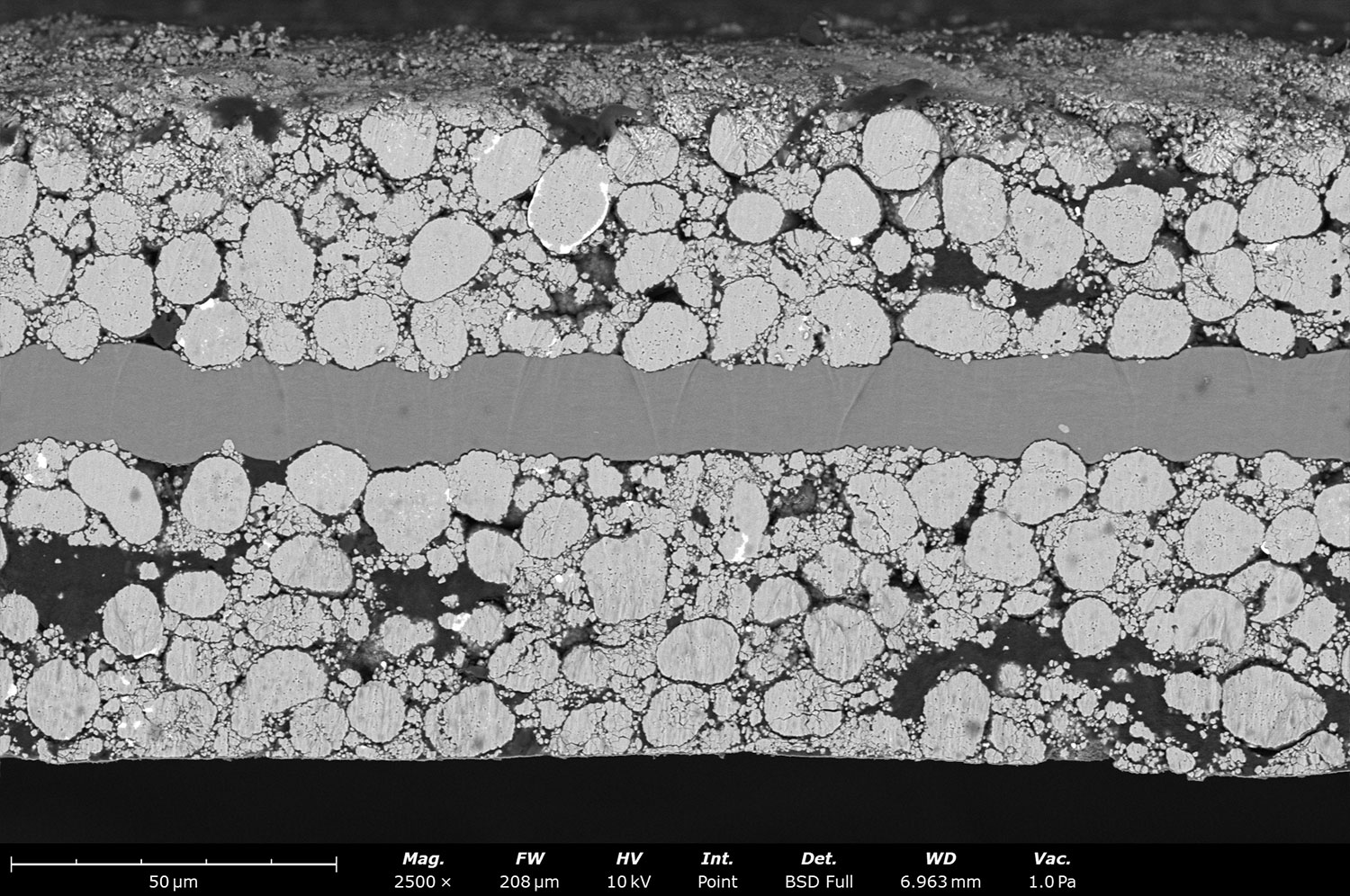
Preparing a specimen for SEM can introduce numerous artefacts onto the surface, such as oxidation, byproducts from processing/manufacturing, or residue from mechanical polishing techniques. An example of a common target for ion mill removal is the Beilby layer, an amorphous surface layer that forms as a result of mechanical polishing. Removing surficial contaminants normally requires other intensive preparation techniques, such as chemical etching. Ion milling, in contrast, can quickly and easily remove these layers from the specimen with limited effort from the operator. Figure 1 compares the cross section of cathode tape after cutting with scissors vs ion milling. The SEM images clearly show the improvement in the quality of the surface after ion beam polishing where details such as particle distribution and layer thickness can be clearly seen. This is the ultimate goal of ion milling; to create a clean, flat surface for high quality analysis. BIB can produce results such as this with limited effort on the part of the operator while simultaneously increasing sample throughput. The following are methods of preparation that are popular using a broad ion beam polishing system:
ABFigure 1. SEM images of cathode tape (a) before ion milling and (b) after sample preparation.
Surface Polishing
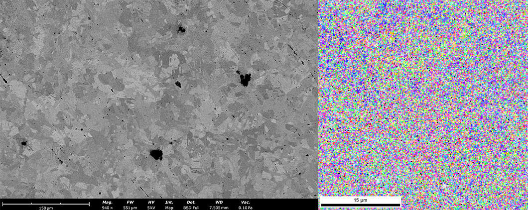
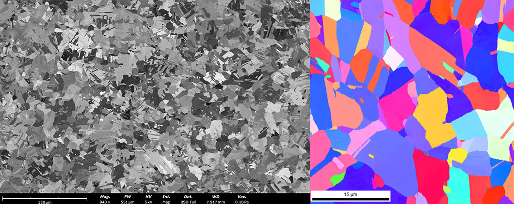
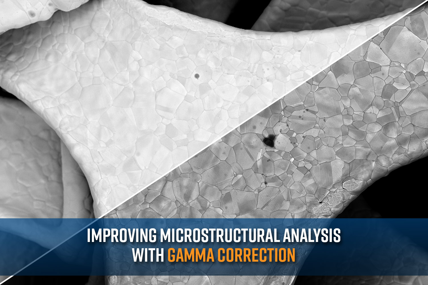
Surface polishing is typically used for flat or epoxy mounted samples to remove a larger portion of the damaged or contaminated layer to create a clean / smooth surface for imaging. One of the most common applications of this technique is to polish the sample surface for EBSD analysis. By polishing metallic or mineral samples, internal crystalline areas, known as grains, can be revealed. Figure 2 compares a sample of copper foil before and after ion mill polishing, both with corresponding EBSD data.1 The grains are immediately identifiable after ion milling and result in a beautiful EBSD mosaic. Analyzing these structures with EBSD reveals much about a sample through analysis of crystal orientation.1 Revealing these grains can be painstaking work with only traditional polishing techniques, especially for hard materials such as high entropy alloys. Ion milling is an ideal technique for these applications as it significantly reduces the workload on the researcher, is more cost effective, and provides higher quality results. Thus, many different industries look to use ion milling for their EBSD sample preparation including those researching semiconductors, batteries, and geologic materials.
ABFigure 2. A comparison of copper foil before (a) and after (b) ion milling with corresponding EBSD data showing the internal crystalline structures of the sample.
Cross-Section Preparation
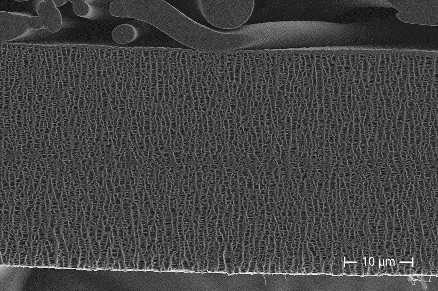
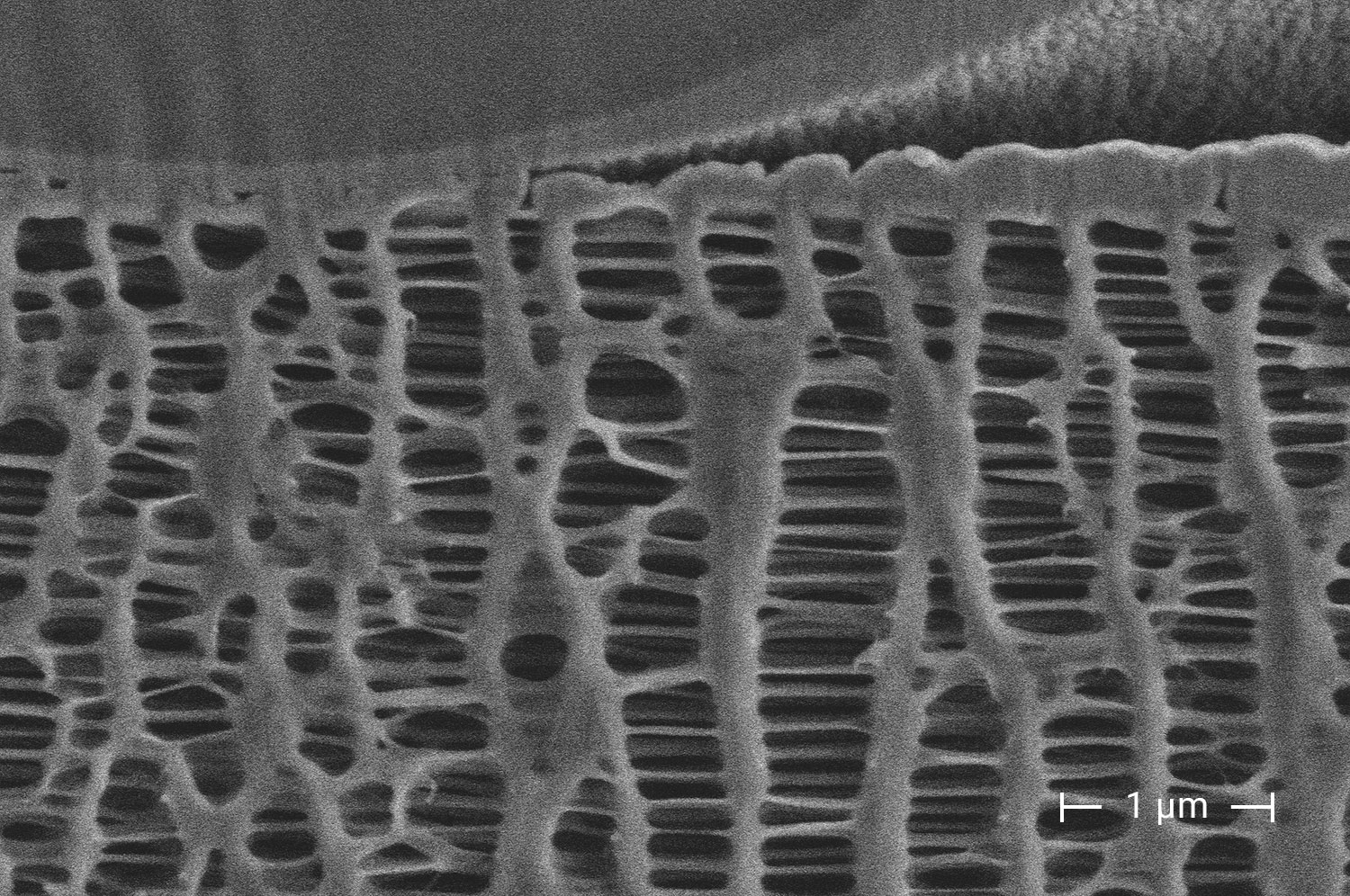
Cross-section preparation is for users looking to target certain areas on a sample to reveal internal structures such as multilayers, interfaces, or failures. Obtaining a cross section reveals the spatial relationship between various components, morphology, and overall composition. As such, cross section analysis is a popular technique across various disciplines. To reveal a cross section, the sample needs to be cut prior to mounting inside an SEM. Depending on the type of cut performed, different artefacts, such as smearing or compressing, can be introduced, leading to poor results. Utilizing an ion mill to cross section samples eliminates these artefacts and reveals the true structures underneath, all while inducing minimal stress and no chemical degradation. Figure 3 shows the SEM image of a battery separator cross section, incredibly sensitive samples that are challenging to prepare properly. Ion milling these samples can result in data showing the true microstructure of the material, all without introducing any chemical alterations or thermal damage. Other specific examples include observing contamination or cracking in cathode powders, measuring fiber cross section diameters, or analysis the crystallographic orientation in metallic components.
ABFigure 3. SEM images of the cross section of a battery separator at different magnifications
Preparation of Electron-Transparent Samples for TEM
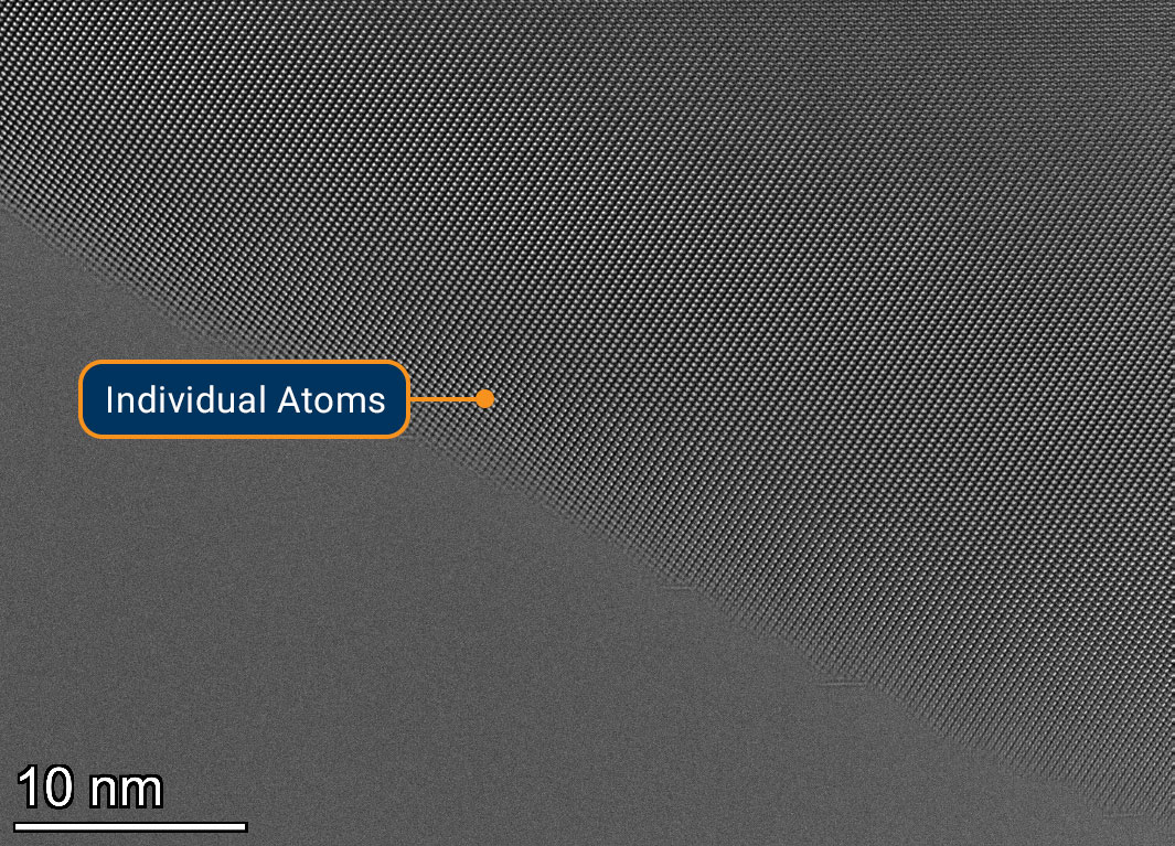
While primarily used for SEM, ion milling also plays a role in preparing samples for transmission electron microscopy (TEM). In TEM, electron transparency is required for imaging, necessitating samples to be thinner than 500 nm. Ion milling is used to achieve this level of precision in preparing thin sections, known as lamellae, for high-resolution microscopy. Monolayers of material are continuously thinned off the sample to achieve atomic-resolution TEM imaging for 2D material research. While traditionally this preparation is achieved using FIB, polishing the lamellae with BIB after the initial cutout can enhance the quality of imaging. BIB provides the operator with the ability to thin the sample with more control and remove any contamination, such as gallium remnants from the FIB. Figure 4 shows an example of BIB polished lamellae and the individual atoms are clearly visible. Performing a low energy polish using a broad ion beam can drastically improve analysis and save both precious time and resources.
Figure 4. Lamellae polished with BIB showing clearly visible atoms
Conclusion
Ion milling is a necessary technique in SEM sample preparation, ensuring high-resolution, artifact-free imaging. By facilitating cleaning of sample surface with various different methods, BIB milling enhances the reliability of SEM analysis across various fields, including materials science, semiconductors, nanotechnology, and forensics. As SEM technology continues to advance, the role of ion milling remains essential in pushing the boundaries of nanoscale imaging and material characterization.
Chen, B., Li, D., Davies, P. et al. Recent Progress of Digital Reconstruction in Polycrystalline Materials. Arch Computat Methods Eng (2025). https://doi.org/10.1007/s11831-025-10245-4↩︎