Introduction
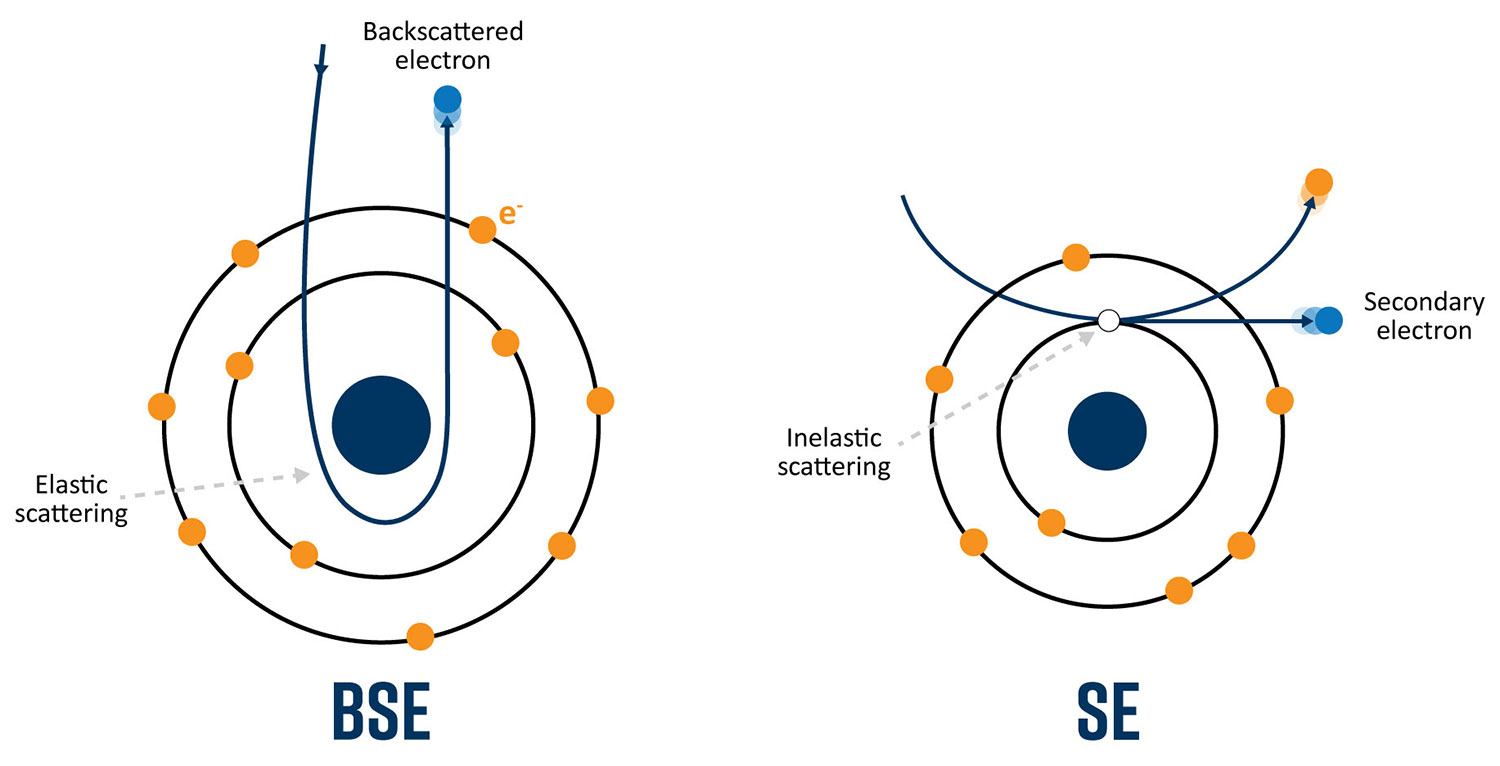
Scanning electron microscopy (SEM) is a technique that employs a focused beam of electrons to scan a surface, point by point, to examine a sample’s surface at high resolution. The interaction of the electron beam with the sample surface results in two different kinds of electrons. Backscattered electrons are high-energy electrons originating from the incident beam of SEM that undergoes elastic scattering with the atomic nuclei of the sample. Secondary electrons are low-energy electrons that are emitted from the surface of a sample when it is irradiated by an electron beam. The beam transfers energy to the atomic electrons through inelastic scattering and ionization, where some of these interactions transfer sufficient energy for the electrons to be ejected from the surface of the specimen. These secondary electrons have relatively low energies, typically on the order of tens to hundreds of electron volts (eV). They possess limited penetration depth into the material and are mostly emitted from the top few nanometers of the sample’s surface.
Different electron detectors are required to collect these two types of electrons generated in an SEM. The selection of an appropriate electron detector is crucial to obtain meaningful data, but it is a choice that depends on the specific research objectives and nature of the sample under investigation. The two types of electron detectors in SEM are:
The Backscattered Electron Detector
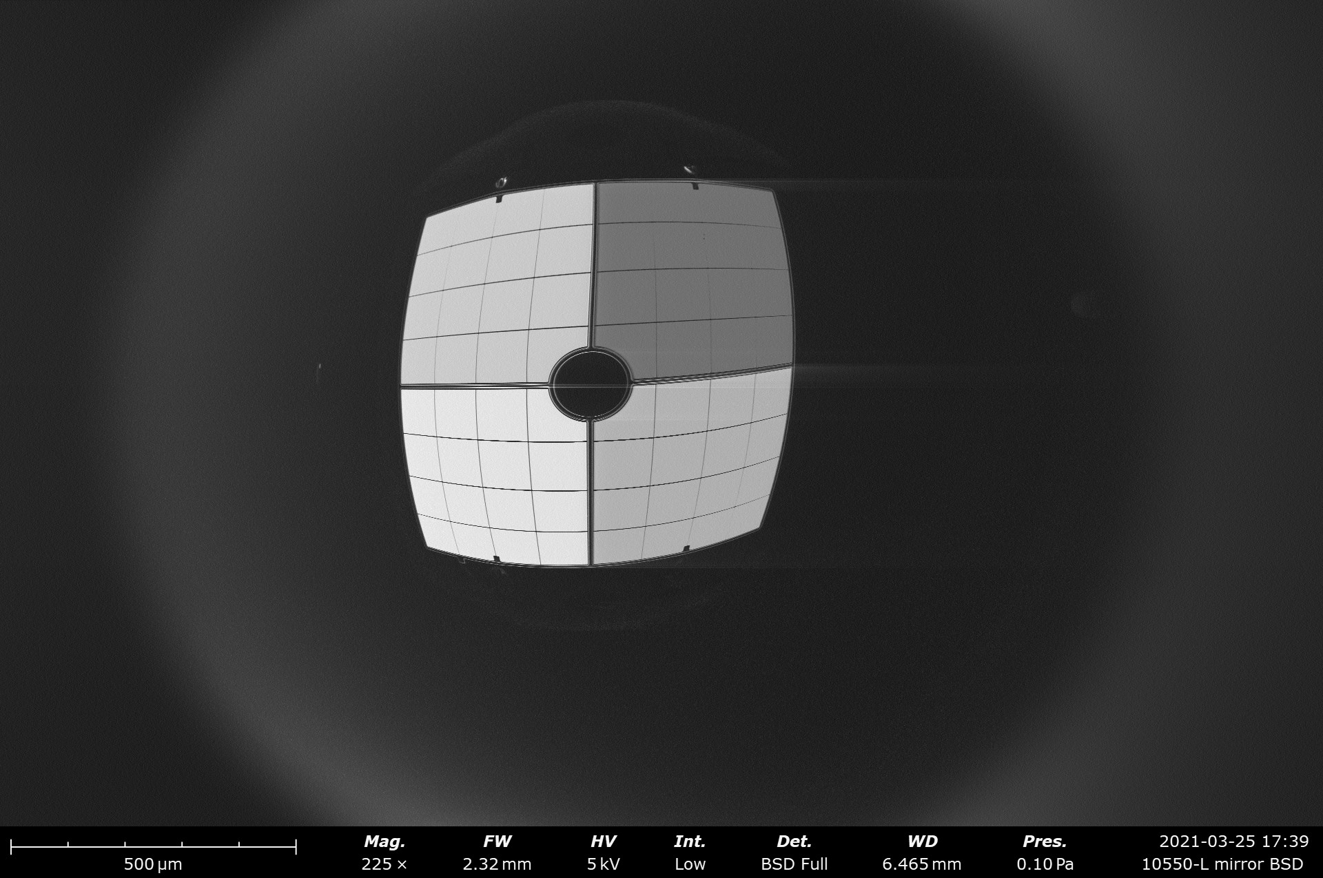
The backscattered electrons are detected using a backscattered electron detector (BSD) placed above the sample. The signals from the detector are then used to generate images that provide compositional and density contrast in the sample.
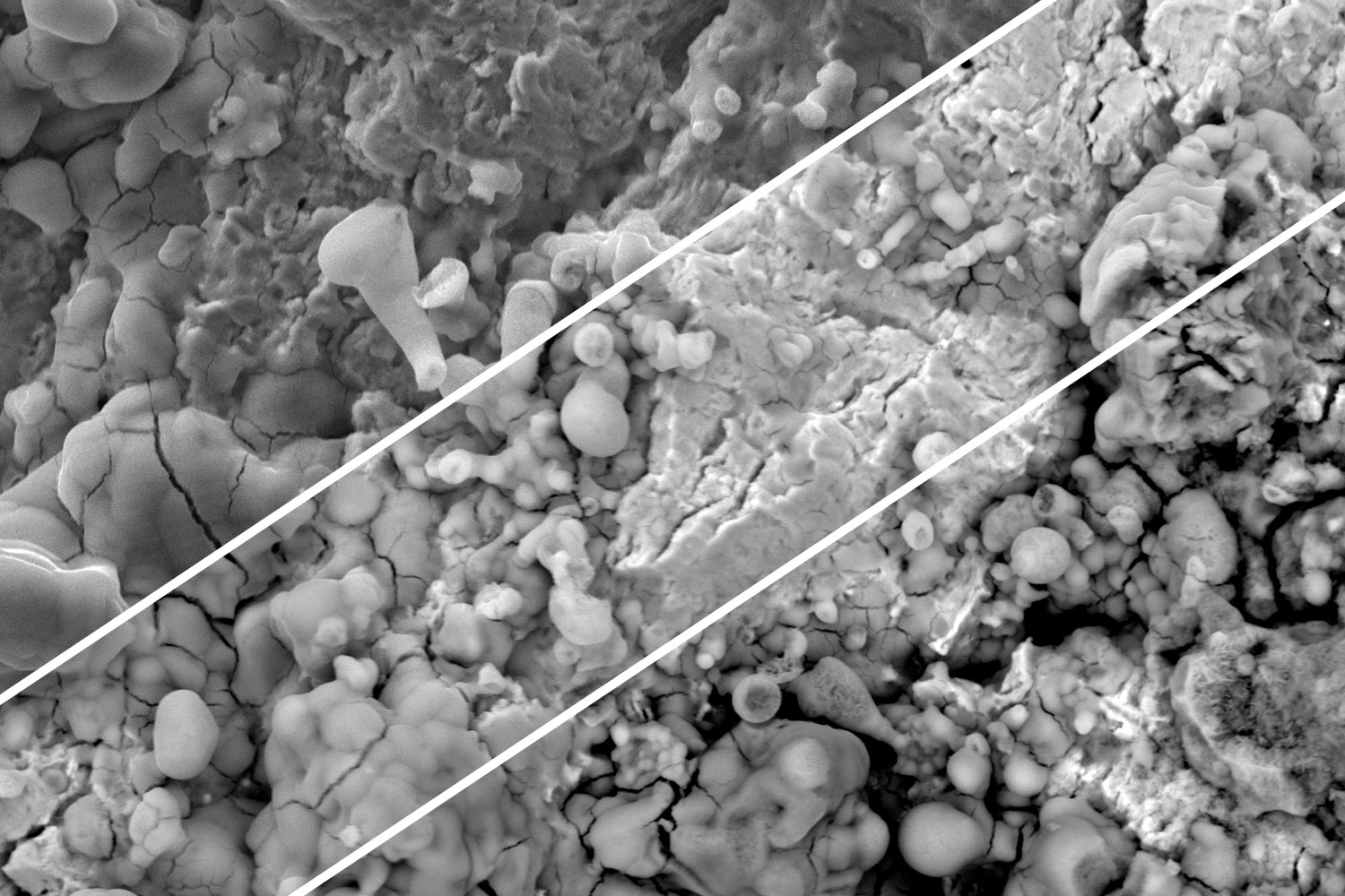
The number of backscattered electrons emitted from the sample depends on the average atomic number at the surface of the sample. Coulomb forces from the positively charged nuclei of the sample cause the backscattered electrons to alter their trajectory, exiting in the “backscattered” direction directly above the region of beam-sample interaction. Regions of an SEM sample containing heavier elements tend to produce more backscattered electrons and brighter contrast in a BSE image than regions containing lighter elements.
In the case of Phenom Desktop SEMs, the solid-state backscattered detector is divided into four separate quadrants. This design maximizes signal to noise and provides flexibility in imaging modes. Standard BSD images can be acquired by activating all four quadrants. By disabling two of the four quadrants and collecting images from opposite sides of the detector, a qualitative topographic image can be generated.

The Secondary Electron Detector
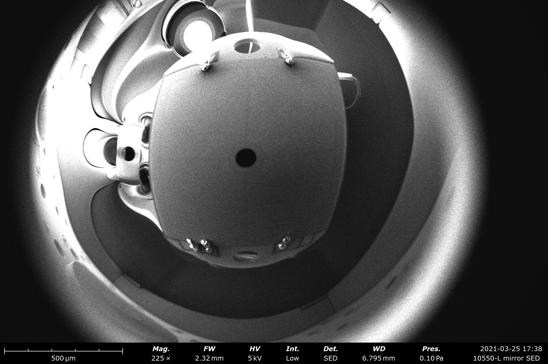
A secondary electron detector (SED) is used to collect the secondary electrons that are emitted from the sample surface and is placed toward one side of the sample chamber at an angle to maximize collection efficiency. Images acquired with the SED are particularly useful for visualizing surface morphology and topography. Because of the smaller interaction volume contributing to SE signal, their images generally demonstrate improved resolution compared to BSD images at the same beam and vacuum settings.
The surface sensitivity of SED imaging also gives rise to a phenomenon called edge effects. At edges and discontinuities on the sample’s surface, more secondary electrons are emitted compared to flat areas. An increased emission enhances the brightness at edges in the resulting images, making the SED valuable for highlighting step edges and other surface features.
Determining Which Detector to Use in SEM
Selecting which detector to use depends on the specific objectives and requirements of the analysis. Some of the main factors to consider when choosing between BSD and SED are:
Surface Sensitivity
If the primary goal is to visualize surface morphology, topography, and fine surface details, the SED is the preferred choice. It provides high resolution imaging to allow for detailed observation of various surface structures and features in detail, capturing electrons emitted from the top few nanometers of the surface.
Elemental Contrast and Composition
If the analysis involves investigating elemental composition and contrast, BSD is a more suitable approach. BSD imaging provides contrast based on the atomic number variations within a sample, making it effective for differentiating materials with different atomic compositions and densities.
Spatial Resolution
The choice of detector may influence the achievable spatial resolution at different accelerating voltages. In general, SED imaging tends to provide higher resolution at lower accelerating voltages because lower energy secondary electrons are less affected by beam broadening due to scattering effects, resulting in sharper images.
Accelerating Voltage
Low accelerating voltages of the electron beam – referred to as low kV imaging (below ~ 10 kV) – is more suitable for SED signals compared to BSD. Some systems, such as the Phenom Pharos Desktop SEM, reach as little as 1 kV for highly sensitive imaging. In backscattered interactions, the signal intensity is reduced when the energy of the incident electrons decreases. The main conclusion to be made is that SED imaging is generally favored for low kV imaging and high-resolution surface details while BSD imaging offers advantages in terms of signal intensity and compositional contrast at higher accelerating voltages.
Conclusion
Both detectors have their own strengths and limitations. In many cases, a combination of BSD and SED imaging is employed to gather complementary information and provide a more comprehensive understanding of the sample. Phenom Desktop SEMs have the unique ability to mix the SED and BSD signals to provide a blended image that is tailored to the user’s level of preference.