Proper assessment of part or surface cleanliness is critical for maintaining the health of mechanics, electronics, and people. While qualitative measurement methods can be adequate for certain applications, verifying technical cleanliness status requires quantitative data. This information can also be used to determine the efficacy of experimental cleaning strategies. Progress in this field can have direct impacts on standards of living, from daily-use product efficiency to surface sanitization and air quality.
Nanoscience Instruments provides the following solutions for your cleanliness needs:
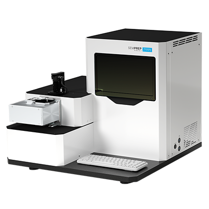
SEMPREP SMART is an automated broad ion milling system featuring two ion sources, low-energy and high-energy. This enables the SEMPREP SMART to have the widest range and highest precision of ion mills on the market. For certain samples, this also eliminates the need for cooling, since they can be milled more gently. Regardless of sample type, the SEMPREP SMART is a great choice for high-quality imaging preparation.
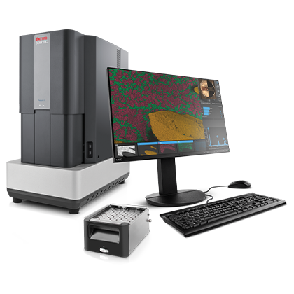
The Phenom line of desktop SEMs hosts the most powerful and reliable electron sources on the market, enabling higher resolutions and magnifications while also reducing maintenance costs. Operators can be trained in a matter of hours, if not minutes, and time-to-image can be as short as 30 seconds. Multiple Phenom models with varying capabilities and sample stages are available to match your analysis needs.
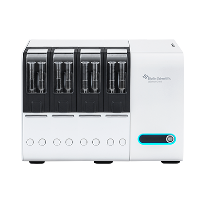
Founded by the original developers of the QCM-D technique, QSense is uniquely equipped to provide top-tier instrumentation to their users. Their technology is more sensitive and easier to use than any QCM instrument on the market, lending value to even the most sensitive and complex experiments. Data analysis can be completed with the accompanying QSoft software.
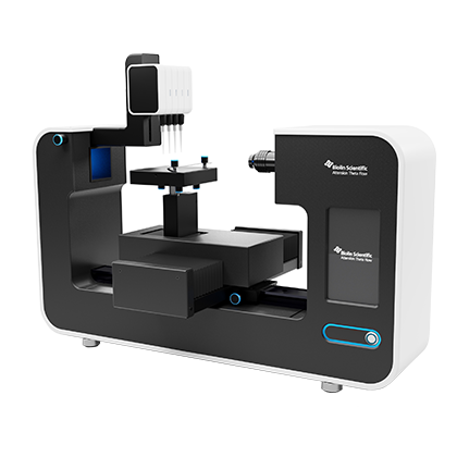
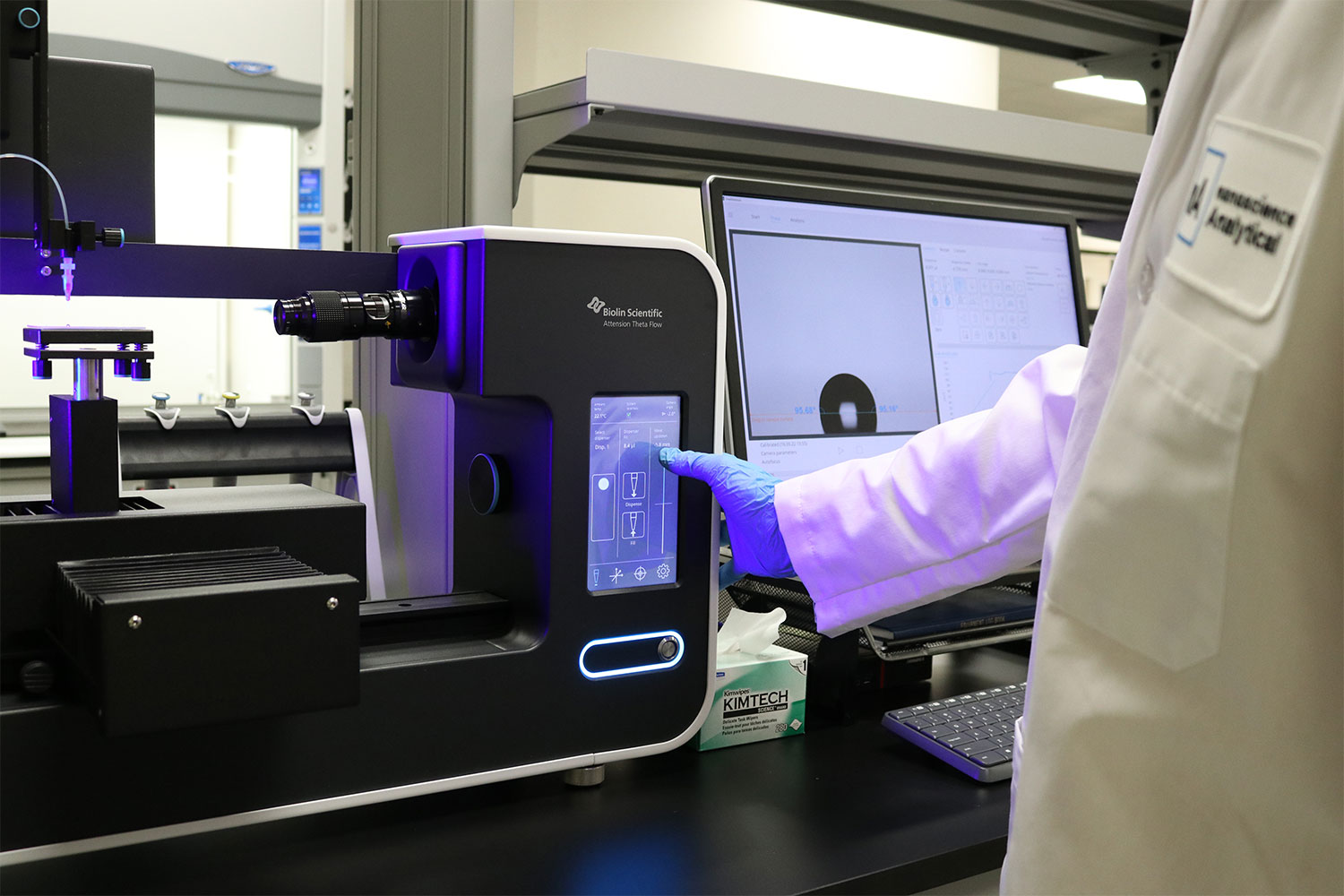
The Attension Theta and Attension Sigma are lines of optical and force tensiometers, respectively. In addition to class-leading hardware and all-inclusive software, the Attension instruments are fully modular, with various plug-and-play accessories available for complex experimentation. The robust instrument design and option to use chemically resistant pipette tips enables use inside of a glovebox and measurements with harsh chemicals.
From benchtop systems to fully automated, industrial-size manufacturing, the Fluidnatek and Spinbox electrospinning systems offer flexibility and scalability for every application. Their focus on environmental control leads to consistency, precision, and efficiency throughout nanofiber production. This is particularly valuable in research applications, where reproducibility is critical for verifying observations and trends.
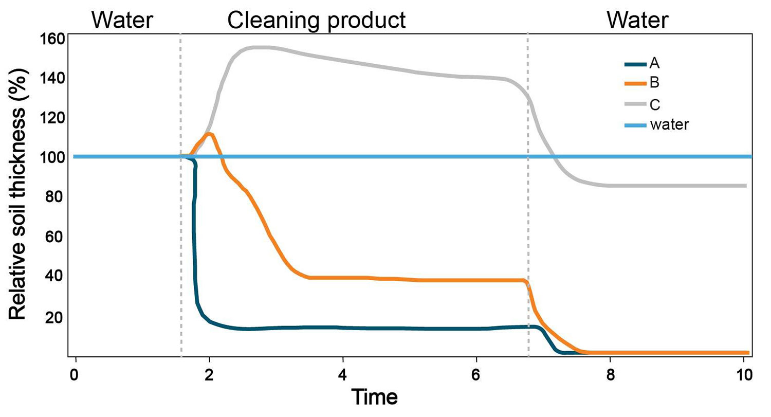
Understanding the dynamic interactions between cleaning agents and hard surfaces provides important insights into cleaning efficiency and areas of improvement. However, many cleanliness assessment methods, such as water break tests, only provide binary pass/fail results. Others can quantitatively assess cleanliness, but only before and after cleaning is performed. Mechanistic information is still not measurable with these techniques.
Quartz crystal microbalance with dissipation monitoring (QCM-D) measures mass and viscoelasticity changes on a sensor surface with time-resolved data. This enables QCM-D to measure features such as stain structure changes or contaminant removal rate, all in real time. Temperature and pH of the sample environment can be manipulated to observe how these parameters affect the cleaning process. Both complete detergents and individual components can be analyzed for cleaning efficacy with QCM-D.
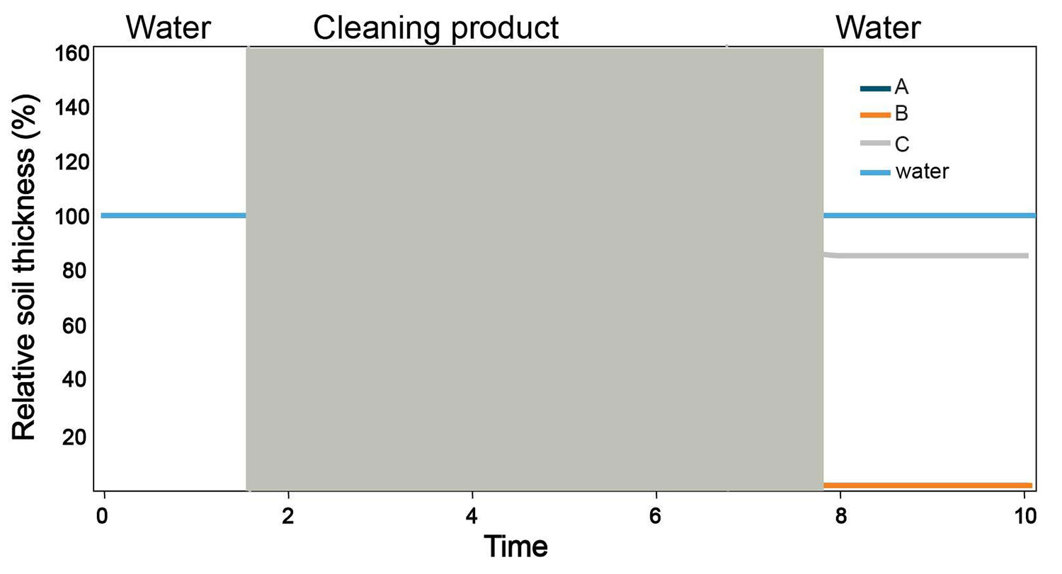
Figure 1. A) Typical outputs for cleaning assessment methods, vs. B) QCM-D outputs.
Cleanliness Solutions
Assessing cleanliness status
Nanoscale contaminant detection
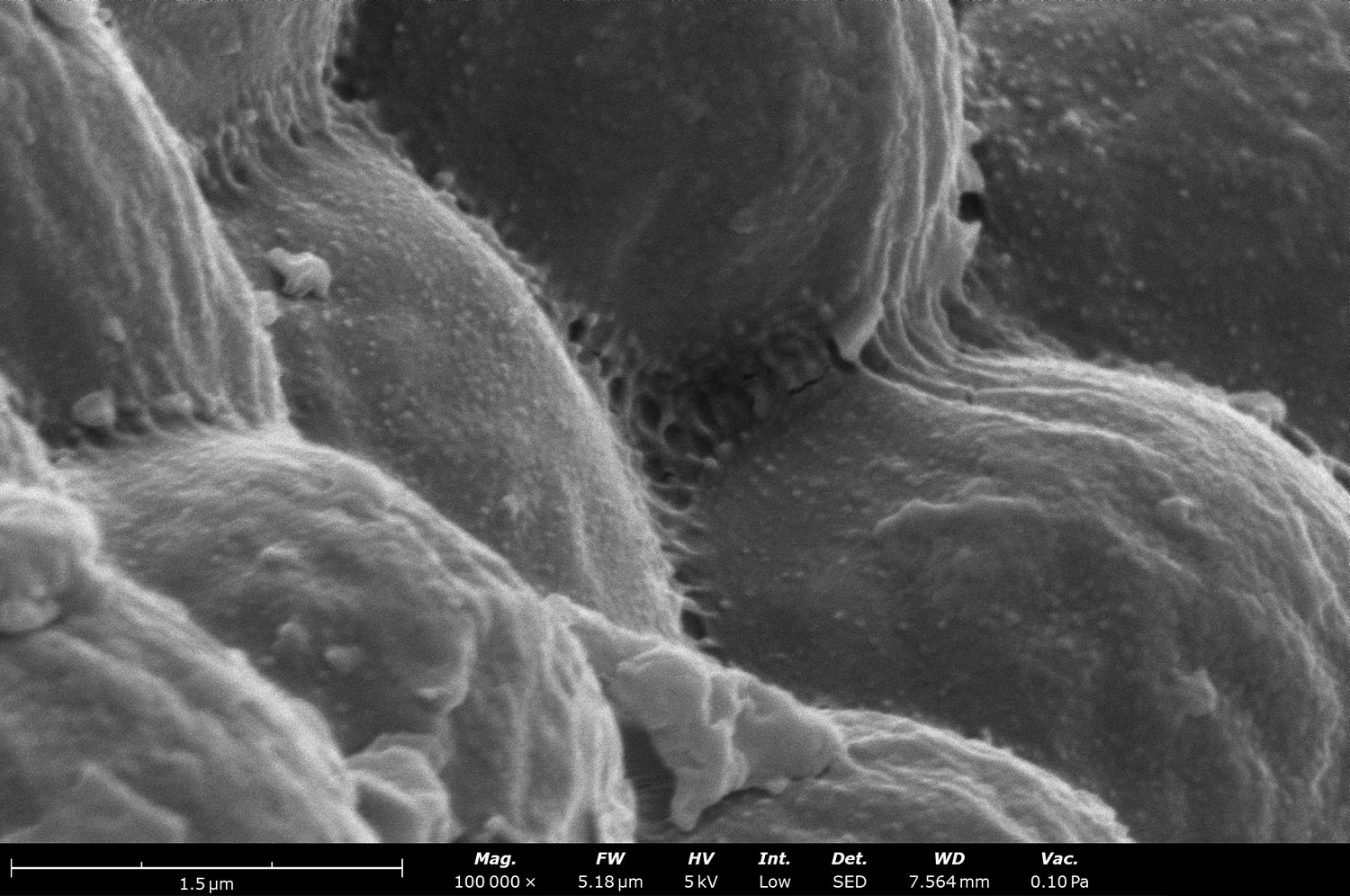
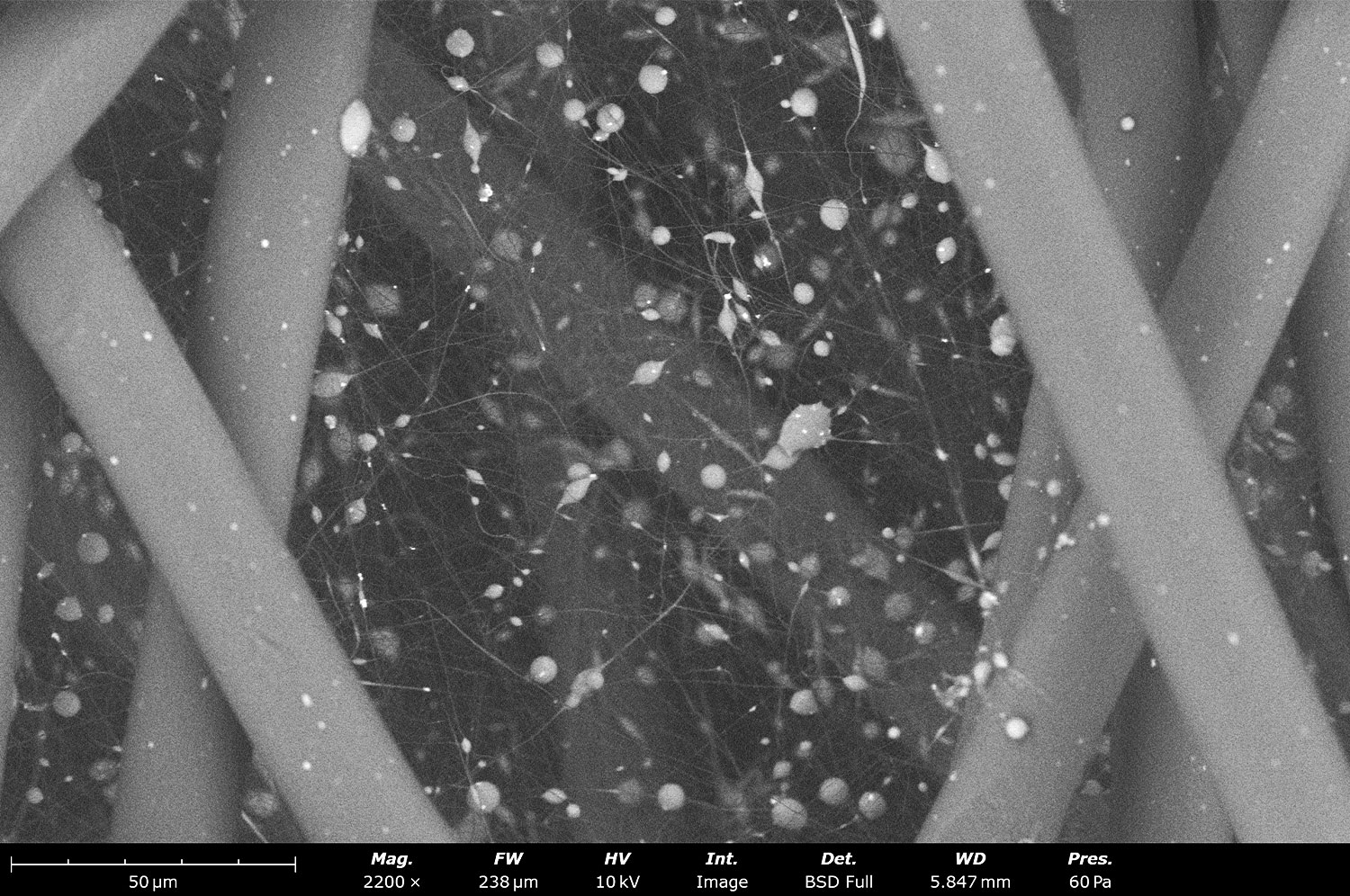
While certain contaminants are visually detectable, and others are only detectable through optical microscopy, some are much smaller; nanoscale particles, despite their size, have the potential to render a product useless or even harmful. This is especially applicable to microelectronics, where individual particles can cause short circuits, and implantable devices, where contaminants could lead to inflammation or infection.
Figure 2. SEM image of coated contaminant particles
Scanning electron microscopy (SEM) utilizes a focused beam of electrons to obtain higher magnifications and resolutions than optical microscopes, enabling detection of much smaller particles. Since the SEM’s backscattered electron detection (BSD) is affected by atomic weight, elemental boundaries can be visualized with contrast on the SEM image, further improving particle detection.
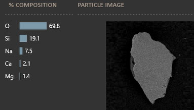
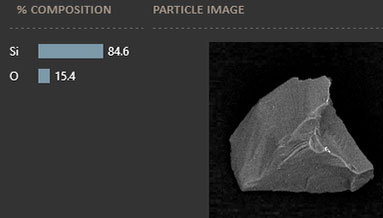
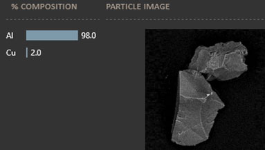
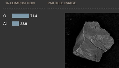
When contamination has been identified, tracking down its source is vital to preventing future cleanliness issues. Particle morphology is useful for this, but without composition information, quantitatively confirming that the contaminant matches its source will be difficult. Therefore, combining SEM technology with energy dispersive X-ray spectroscopy (EDS), which uses characteristic X-rays to determine elemental composition, is ideal for determining contaminant sources. Particles can be identified morphologically and elementally, then compared to particles from the environment or any production tools used to machine the part. This lowers the risk of future contamination events.
Figure 3. Possible contaminant particles analyzed with SEM-EDS using a ParticleX TC desktop SEM.
Quantification of surface free energy
One indicator of a surface’s cleanliness is wettability; surfaces with better wetting are usually considered to be cleaner. Other methods of cleaning have binary pass/fail results or require time-intensive measurement techniques that are unsuitable for many applications.
Tensiometers, which analyze surface and interfacial tension, can characterize wettability with a single water contact angle measurement. Optical tensiometers are ideal for this, since they tend to be faster than force tensiometers. Both instruments are quick, nondestructive, and quantitative, lending greater insights into the true cleanliness of a surface. Standards such as ASTM C813-90 outline methods for testing for contamination with contact angle measurements. Contact angle measurements have also been used to characterize self-cleaning surfaces.1
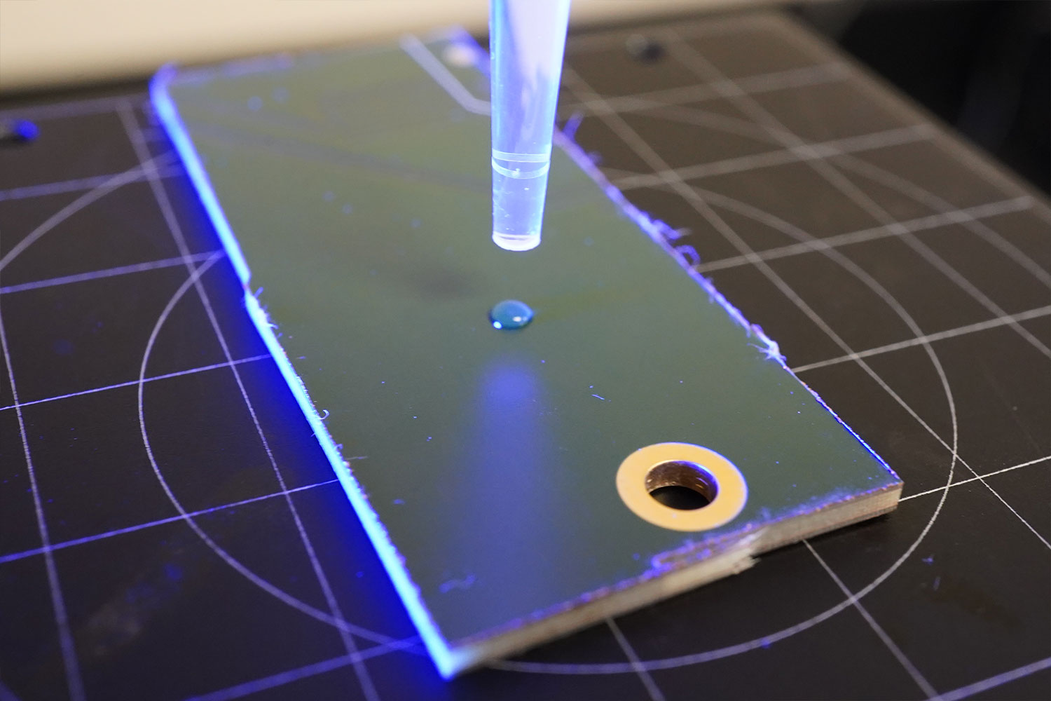
In many cases, a single water contact angle measurement is adequate for assessing cleanliness. For more accurate wettability quantification, or in cases where water would damage the sample, the surface free energy (SFE) can be calculated, which combines contact angle measurements from multiple probe liquids. In scenarios where static or sessile drop measurements are not possible, including analysis of single fibers or very small samples, force tensiometers can help quantify SFE.
Figure 4. A) Operating the Theta Flex optical tensiometer and B) setting up water contact angle analysis on a sample.
Cleanliness Solutions
Optimizing the cleaning process
Nanofiber filter fabrication
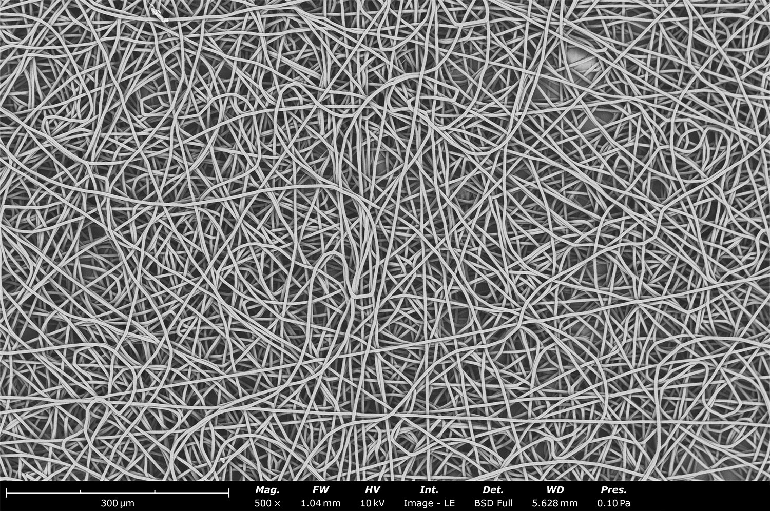
For air and water purification applications, nanofibrous membranes are known to reliably filter out particulate matter or toxic gases.2 There are various options for nanofiber fabrication methods, such as self-assembly and template-based synthesis, but electrospinning is unique due to its high efficiency and ability to tune material properties. Since electrospinning can accommodate a wide range of materials and fiber structures, it is a particularly valuable technique for developing filter membranes with new and improved properties. Innovations like these have the potential to directly improve public health and safety.
Figure 5. SEM image of filtration media fabricated with electrospinning
Surface cleaning of microelectronics
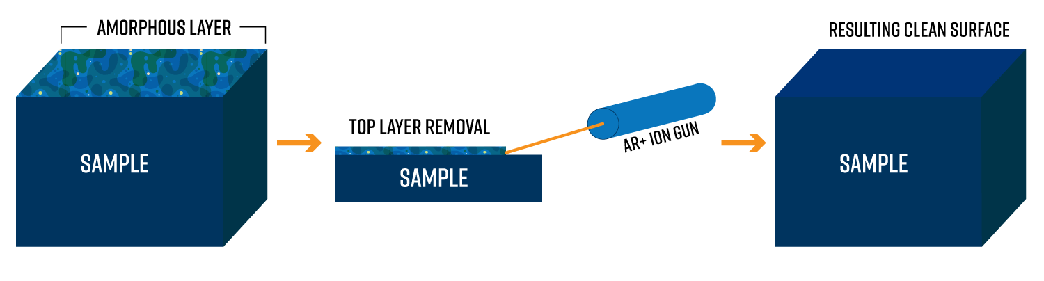
When fabricating complex and precise structures such as integrated circuits, cleaning must be performed regularly to ensure proper function. Foreign particles can cause device-ruining complications; naturally, high-precision cleanliness is required to ensure semiconductor quality. Typically, this is done with chemical mechanical planarization (CMP), which removes material with chemical slurry and mechanical abrasives until the desired features are exposed. However, mechanical polishing often leaves an amorphous layer, called the Beilby layer, on the remaining surface. Broad ion beam (BIB) polishing, which uses the kinetic energy of an ionized argon beam to precisely and uniformly remove material from a sample’s surface, can remove this layer, resulting in a clear and accurate cross-section.
Figure 6. Process of removing the amorphous layer with broad ion beam polishing
Removing individual contaminants from small or delicate components, such as vias, has historically been done through wet chemical etching or reverse sputtering.3 These methods must be carefully controlled to preserve the physical, chemical, and electronic properties of the wafer. Alternatively, ion milling can be used to precisely remove contaminants with minimum effects on the rest of the component. This enables cleaning for a much wider range of components that may be too sensitive for other methods.
Figure 7. SEM image of a semiconductor cross section before and after BIB milling
Cleanliness Solutions
Maintaining cleanliness standards
Automation for technical cleanliness
Assessing technical cleanliness (TC) in mass production scenarios is often tedious and presents challenges for reproducibility. Manual operation also increases the time needed to image and assess each sample. Automation software, by enabling custom thresholds for size, elemental contrast, and other properties, removes the chance of user bias. The time required to obtain an actionable pass/fail report is significantly shortened, which increases throughput potential. Software can also assist with damage prevention by enabling careful monitoring of contamination levels before thresholds are met.
Ragesh, P.; Ganesh, V. A.; Nair, S. V.; Nair, A. S. A review on ‘self-cleaning and multifunctional materials.’ Journal of Materials Chemistry A2014, 2 (36), 14773–14797. https://doi.org/10.1039/c4ta02542c. ↩︎
Lyu, C.; Zhao, P.; Xie, J.; Dong, S.; Liu, J.; Rao, C.; Fu, J. Electrospinning of nanofibrous membrane and its applications in air filtration: a review. Nanomaterials2021, 11 (6), 1501. https://doi.org/10.3390/nano11061501. ↩︎