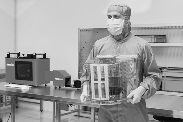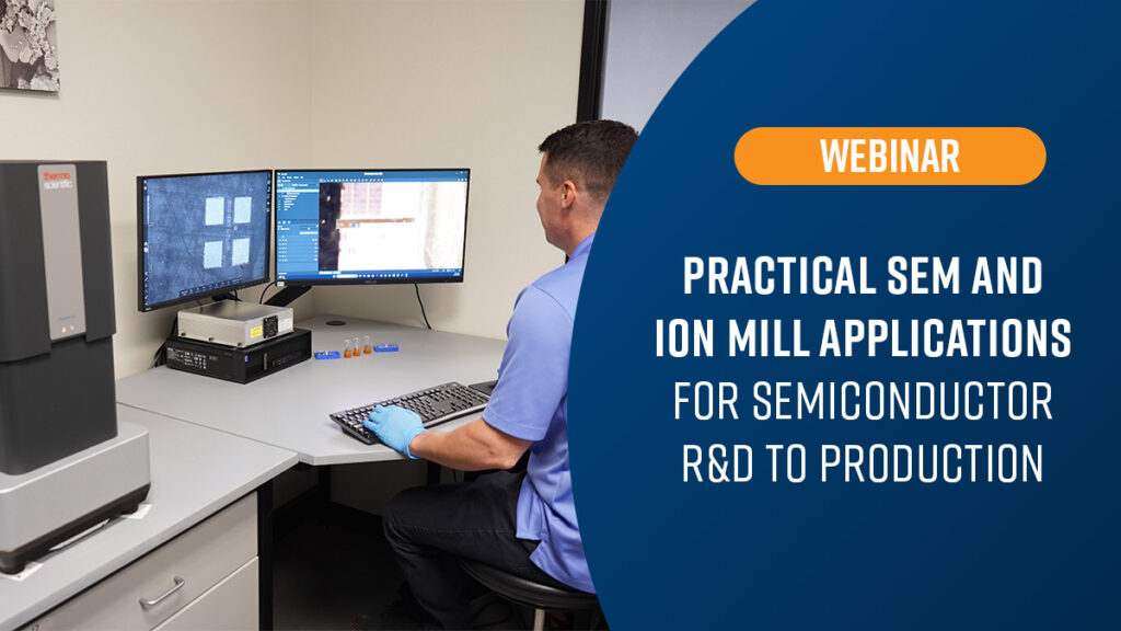
Scanning Electron Microscopes (SEMs) and Cross-sectioning/Polishing tools play a vital role in semiconductor development, from initial materials research to quality assurance in production. Our upcoming webinar will explore how SEMPREP SMART broad ion beam (BIB) milling systems and the Phenom benchtop SEMs can streamline sample preparation and imaging throughout the semiconductor lifecycle.
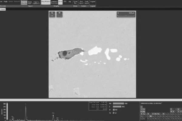
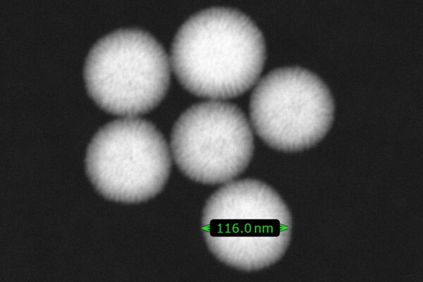
You will learn how the SEMPREP SMART Ion Mills enable precise cross-sectioning and polishing of multilayer semiconductor structures while minimizing curtaining and beam damage, ensuring accurate subsequent characterization of interfaces and critical dimensions. We will demonstrate how Phenom SEMs deliver high-resolution surface and cross-sectional imaging in a walk-up platform, enabling rapid defect detection, surface analysis, and layer thickness evaluation. Finally, we will conclude by discussing how automated imaging workflows and software solutions reduce operator bias and enhance throughput, making Phenom SEMs an ideal solution for demanding R&D labs.