Introduction

Why SEM Is Essential for Semiconductor QA, QC, and FA
Modern semiconductor devices feature critical dimensions well below the limits of optical inspection methods. SEM provides nanometer-scale resolution, enabling visualization of fine details such as line edge roughness (LER), critical dimension (CD) variations, contact and via integrity and gate and interconnect profiles. This level of detail is essential for identifying subtle process deviations before they impact yield or device performance.
SEM imaging is also highly sensitive to surface morphology and compositional differences which allow engineers to distinguish between layers, interfaces, voids, residues, and defects that may be invisible to other techniques.
During process development, SEM is used to establish baselines and validate process capability. Typically, SEM is used in QA to verify pattern fidelity after lithography and etching, measure CDs and profile shapes, evaluate new materials, films, and deposition processes and establish reference images for known good structures. By providing early and accurate feedback, SEM helps ensure that new processes meet design and reliability requirements before scaling up to production.
In high-volume manufacturing, SEM supports ongoing monitoring of process stability and consistency. Common QC use cases include routine CD measurement and trend analysis, detection of systematic defects such as bridging, breaks, or pattern collapse, and monitoring uniformity across wafers and lots.
When devices fail electrically or mechanically, SEM plays a central role in identifying root causes. SEM in failure analysis typically involves high-magnification SEM imaging to identify physical anomalies, cross-sectional analysis to examine buried structures and identifying defects such as voids, cracks, delamination, or process-induced residues. SEM-based FA provides direct visual evidence that links failures to specific process steps, materials, or design features, enabling targeted corrective actions.
Why Sample Preparation Matters in Semiconductor SEM Analysis
Modern semiconductor devices contain ultra-thin films, high-aspect-ratio structures, and buried interfaces that are highly sensitive to mechanical stress, contamination, and beam damage. Improper preparation can distort or damage these features, masking true process conditions or creating misleading artifacts. This is particularly important for root cause analysis, where subtle structural changes may distinguish between process-induced and use-induced failures.
Many critical defects in semiconductor devices occur below the surface, within interconnect stacks, vias, or transistor channels. SEM analysis of these regions requires precise exposure of targeted areas without damaging surrounding structures. Various methods exist to reveal these key attributes, with the simplest and most common involving sectioning via a cutting tool (diamond saw, scribe, etc.) and then mechanically grinding until said feature is revealed. While effective at processing large-scale features of interest, this method of preparation isn’t particularly precise at the nanoscale and can easily damage delicate structures. The continuous miniaturization of these components has made it even more difficult to properly prepare with just cutting and grinding. More advanced preparation methodologies are needed for inspection at the nanoscale, such as ion beam processing.
Ion beam polishing, or ion milling, is typically the final step in the mechanical preparation process. It operates by accelerating a beam of ionized, inert gas towards a sample, and the consistent bombardment of this ion beam sputters material away from the surface, revealing the structure underneath. This methodology preserves the true features of the sample while removing any artefacts introduced from mechanical preparation, such as scratches and contamination. The most popular application of this ion milling is focused ion beam (FIB) processing, which relies on mounting a FIB column onto an SEM to perform site-specific material removal at the nanoscale. These are often referred to as dual-beam SEMs or FIB-SEM. The prevalence of FIB in the semiconductor world is certainly justified, as it solves a lot of problems that traditional mechanical preparation cannot and reveals far more about hidden structures. While FIB excels at these nanoscale applications, it does struggle when trying to reveal large areas on a sample, thus resulting in extended queue times and impeding analysis. Many laboratories look to offload some of the work from the dual beams and broad ion beam (BIB) polishers offer a great solution.
Broad Ion Beam Milling as an Effective Sample Preparation Tool
BIB polishers are stand-alone, compact instruments that rely on a broad-area, low energy argon ion beam for sample preparation. This approach minimizes amorphization and ion implantation, preserves delicate interfaces and thin films, while reducing beam-induced artifacts that can obscure true failure mechanisms. BIB-milled surfaces are exceptionally smooth and free of mechanical damage, which directly improves SEM image quality (Figure 2). These systems are simple to use and require minimal maintenance, making them an excellent choice for any laboratory conducting qualitative inspection and quantitative metrology.
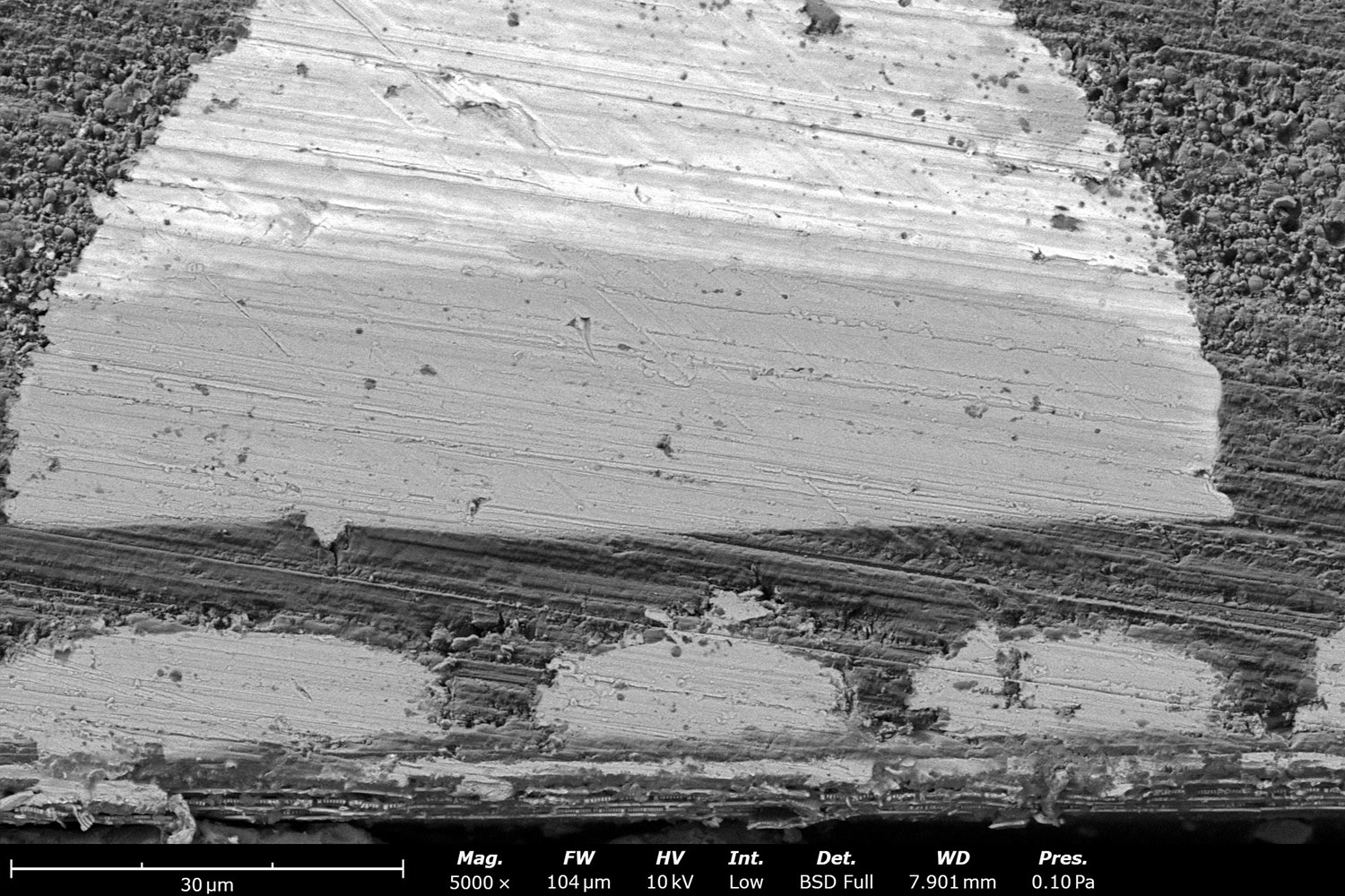
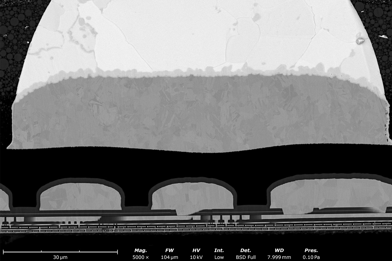
Figure 2. (A) Mechanical polishing results in pronounced mechanical damage, surface roughness, and smearing those obscure true microstructural features. (B) After broad ion milling, the cross-section exhibits a smooth, damage-free surface with clearly resolved layer interfaces and improved contrast, enabling accurate structural and defect analysis.
SEMPREP SMART: The BIB milling system for Semiconductor SEM Sample Preparation
The SEMPREP SMART broad ion beam (BIB) milling system is engineered specifically to deliver high-quality, damage-free surfaces that maximize the value of subsequent SEM imaging and analysis. SEMPREP SMART, designed by Technoorg Linda, is the culmination of the company’s vast experience with broad ion beam sample preparation stretching over 30 years (Figure 3). A combination of gentle, yet powerful, ion sources coupled with a ±1 µm precision stage and dedicated holders to accommodate various sample types, ensures the highest quality of SEM sample preparation.
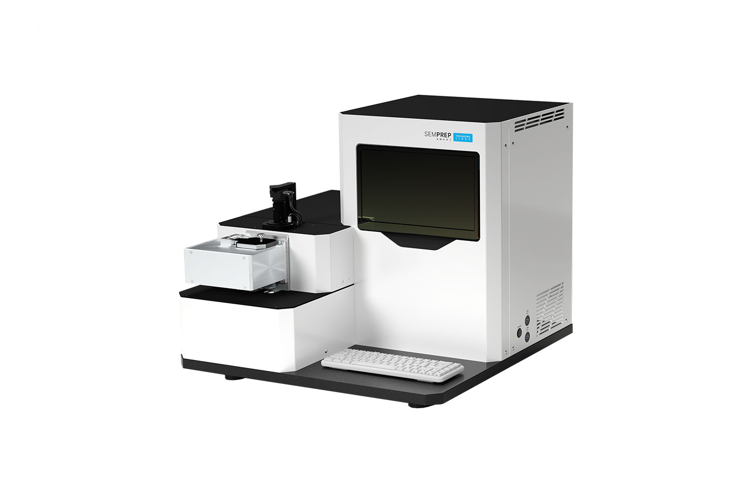
Precise sample positioning is one of the many highlights of FIB milling and it’s part of the reason the SEMPREP SMART stands out among broad ion polishers. Achieving a cross section on a component using BIB polishing has, traditionally, required a substantial amount of effort and was not always consistent. SEMPREP SMART bridges that gap thanks to its precise sample stage and it’s accompanying digital microscope, the Sample Alignment Station (SAS). The workflow of mounting samples for cross sectioning in the SAS is extremely precise, within ±1 µm, and is optimized for direct targeting of a desired feature. Samples are then directly loaded into the SEMPREP SMART, where the automatically aligned stage ensures the strongest part of the ion beam hits the sample.
The gentle nature of the SEMPREP SMART ion beam also minimizes the localized heat load exerted on the sample, in many cases circumventing the need for active cooling. Delicate structures that traditionally require cooling, such as Printed Circuit Boards (PCBs), are thus not altered by exposure to the beam, hastening the overall milling time. Particularly sensitive samples, such as Liquid-Crystal Polymers (LCPs), may still require active cooling but with the SEMPREP SMART, the extent required is minimal. LCPs would traditionally require LN2 cooling but with the SEMPREP SMART, Peltier cooling can be employed instead which is simpler to both use and maintain.
Both the precision staging and cooling capabilities of SEMPREP SMART are controlled by a user-friendly control software with automated alignments, recipe-based workflows, and process automation. These capabilities reduce operator variability and accelerate throughput in environments where high sample volumes or consistent results are required. Laboratories exploring novel materials or consistently investigating batches of known products can easily employ the optimal milling parameters to ensure the best possible results.
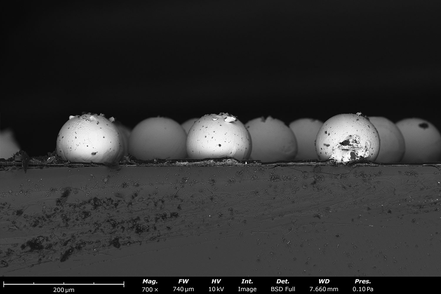
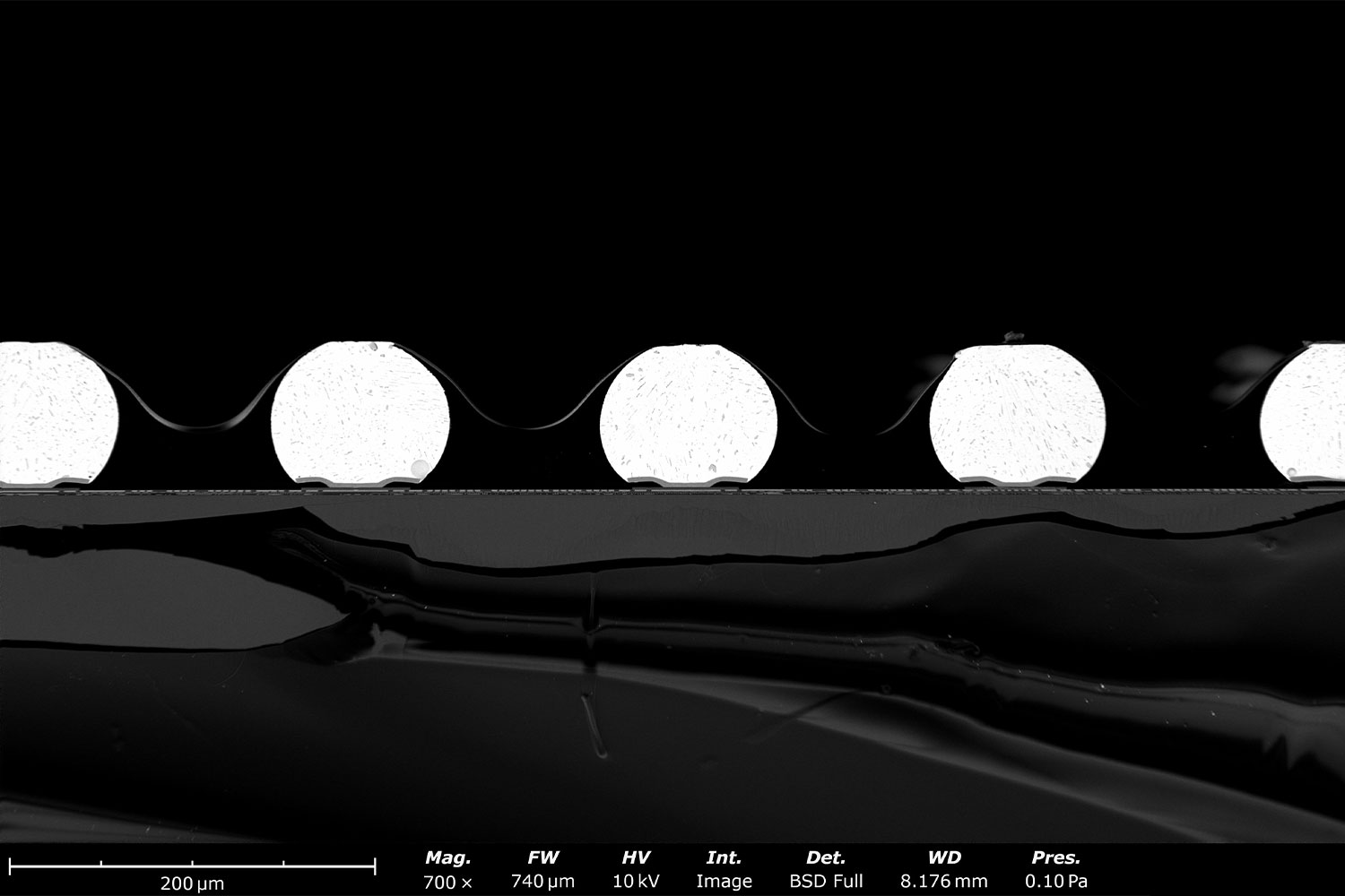
Figure 4. SEM images of pre-milled (A) and BIB milled (B) solder balls. The pre milled samples shows the effects of the mechanical sample preparation,
obscuring the interface between the solder balls and the adjoining surface. The images of BIB milled sample clearly show the interface.
Key Takeaways
Scanning Electron Microscopy is a cornerstone technology for QA, QC, and Failure Analysis in semiconductor manufacturing. Its high-resolution imaging, sensitivity to topography and materials, and compatibility with automation make it uniquely suited to the demands of advanced device nodes.
Sample preparation is a critical enabler of effective SEM-based QA, QC, and failure analysis in semiconductor manufacturing. It directly impacts image quality, measurement accuracy, and the reliability of conclusions drawn from SEM data. Broad ion beam milling is a highly effective sample preparation technique for SEM-based QA, QC, and failure analysis in semiconductor manufacturing since it preserves nanoscale features and interfaces while minimizing artifacts. It also produces large area representative cross-sections that enable access to buried structures essential for failure analysis. The SEMPREP SMART broad ion beam milling system delivers a combination of precision, automation, and flexibility tailored to the demanding requirements of semiconductor SEM sample preparation.
References
- Amato, U.; Antoniadis, A.; De Feis, I.; Doinychko, A.; Gijbels, I.; La Magna, A.; Pagano, D.; Piccinini, F.; Suviseshamuthu, E. S.; Severgnini, C.; Torres, A.; Vasquez, P. Detecting Important Features and Predicting Yield from Defects Detected by SEM in Semiconductor Production. Sensors 2025, 25 (13), 4218. https://doi.org/10.3390/s25134218. ↩︎
- Gholinia, A.; Curd, M. E.; Bousser, E.; Taylor, K.; Hosman, T.; Coyle, S.; Shearer, M. H.; Hunt, J.; Withers, P. J. Coupled Broad Ion Beam–Scanning Electron Microscopy (BIB–SEM) for polishing and three dimensional (3D) serial section tomography (SST). Ultramicroscopy 2020, 214, 112989. https://doi.org/10.1016/j.ultramic.2020.112989. ↩︎
- Zhou, S.; Lin, Z.; Qiu, B.; Wang, H.; Xiong, J.; He, C.; Zhou, B.; Pan, Y.; Huang, R.; Bao, Y.; Cai, N. Evaluation of Solder Joint Reliability in 3D Packaging Memory Devices under Thermal Shock. Electronics 2022, 11 (16), 2556. https://doi.org/10.3390/electronics11162556. ↩︎