Decoding the Best Phenom SEM for Your Needs

Scanning electron microscopy (SEM) is an incredibly adaptable analytical method that generates high-resolution images by scanning a focused electron beam across the surface of a sample. Inside the SEM instrument, a range of detectors captures various signals produced during the interaction between the electron beam and the sample, enabling the visualization of surface microstructure and elemental composition. Compared to optical microscopes, the exceptional resolving capacity of SEMs establishes them as an essential instrument across numerous industries, particularly those working with functional materials.
Igniting Young Minds: How Whitesboro High School Brought Nanotechnology to Life

Imagine being able to visually explore the nanoscale structures of bugs, pollen, cells, minerals, and more. To zoom thousands of times closer than the naked eye and study intricate details spanning just billionths of a meter. A scanning electron microscope (SEM) is a versatile tool which makes use of an electron beam to scan the surface of a sample to make this vision an achievable reality. Making sense of such small scales requires grasping dimensions exponentially smaller than our direct experience, and an SEM provides a powerful lens to explore these landscapes.
The Advanced Materials Show 2023 | Oct. 3-4, 2023 | Columbus, OH

Nanoscience Instruments cultivates global partnerships to deliver cutting-edge electron microscopy, surface analysis, and material characterization solutions. Visit our booth for live, hands-on demonstrations of industry leading Tensiometers and automated desktop Scanning Electron Microscopes (SEMs). These unique instruments enable transformative advancements in materials development and manufacturing workflows for optimizing your next-generation materials.
10 Reasons to Use Electrospinning

Electrospinning is a voltage-driven material fabrication process that can be used to produce micro to nano-scale fibers. The electrospinning process is a combination of interacting electric, hydrodynamic, and surface tension forces resulting in “electrohydrodynamic phenomena” which affect the electrospinning solution as a high voltage is applied. The most common basic setup involves a spinneret, high voltage source, material (e.g., polymer) in solution within a reservoir, and a grounded or charged collector.
The Battery Show 2023 | Sept. 12-14, 2023 | Novi, MI

Nanoscience Instruments provides solutions for battery development applications through cutting-edge instrumentation and analytical services. Visit our booth for live demonstrations of desktop SEM with automated workflows designed for structural and chemical analysis of battery materials, and learn about our surface characterization tools, battery cyclers & potentiostats, and process development and analytical services.
Why is Camera Resolution important in Optical Tensiometry?
An optical tensiometer, also known as a contact angle goniometer, is an instrument used to characterize material surface properties and interactions between liquid and solid phases. In the simplest experiments, the optical tensiometer places a drop of liquid on the surface and records and analyzes the shape of the drop. The tendency of the drop to spread across the surface is a function of the surface tension of the liquid, gravity, the difference in density of the sample liquid and its surrounding medium, and the properties of the solid surface. Optical tensiometers are used in many industries and scientific disciplines to collect a wide variety of surface measurements, including contact angle, roll-off angle, surface free energy, surface tension, and interfacial tension, among others. The contact angle measurement carried out with an optical tensiometer is the most extensively used method to characterize and quantify the wetting properties of a surface.
Which Electron Detector is Right for Your Application?
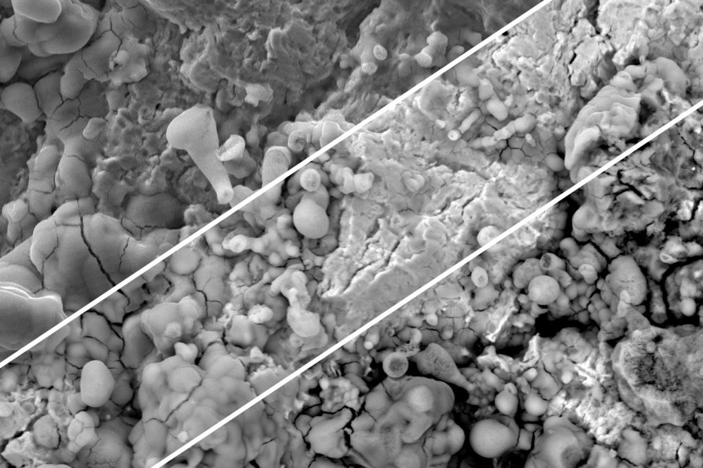
Scanning electron microscopy (SEM) is a technique that employs a focused beam of electrons to scan a surface, point by point, to examine a sample’s surface at high resolution. The interaction of the electron beam with the sample surface results in two different kinds of electrons. Backscattered electrons are high-energy electrons originating from the incident beam of SEM that undergoes elastic scattering with the atomic nuclei of the sample.
8 Reasons to Buy a Commercial Electrospinning or Electrospraying System
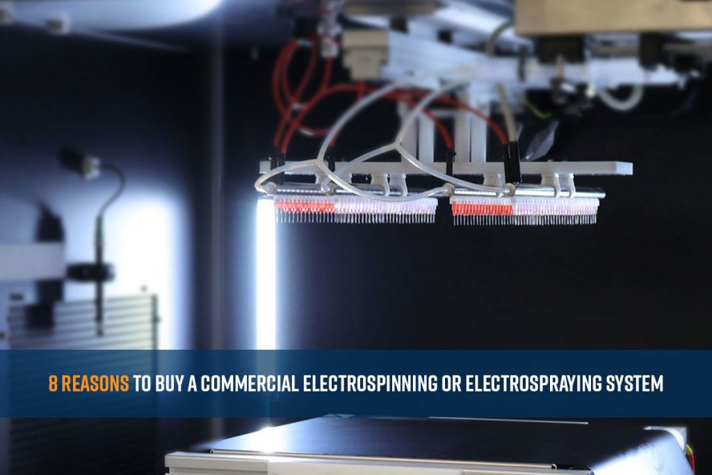
Electrospinning and electrospraying are electrohydrodynamic processes wherein a polymer solution is used to fabricate fibers or particles, respectively. In the most basic setup, a polymer solution is loaded into a syringe, and it flows through a capillary tube where a high voltage is applied, and the liquid is ejected towards a collector. Depending on the solution properties, fibers or particles are generated during the process.
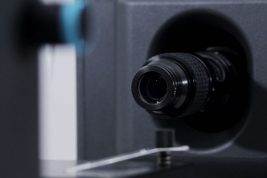
5 Reasons to Purchase a Scanning Electron Microscope (SEM)
In the domain of scientific research and advanced industrial applications, the scanning electron microscope (SEM) is a powerful tool that has revolutionized our understanding of the microscopic world. Its exceptional imaging capabilities and analytical features have made it an indispensable instrument for various applications pertaining to materials science and life sciences. In this blog post, we will explore five compelling reasons why investing in a scanning electron microscope can be highly advantageous.
Controlled Release Society | July 24-28, 2023 | Las Vegas, NV

Controlled Release Society 2023 Annual Meeting Nanoscience Instruments/Nanoscience Analytical provide instrumentation and process development solutions that satisfy the R&D demands of drug delivery applications. Visit Booth #404 to witness how our ISO-certifiable electrospinning equipment enables encapsulation of APIs or creation of biomimetic structures including grafts and tissue scaffolds. Afterwards, characterize the products with our automated […]