In the domain of scientific research and advanced industrial applications, the scanning electron microscope (SEM) is a powerful tool that has revolutionized our understanding of the microscopic world. Its exceptional imaging capabilities and analytical features have made it an indispensable instrument for various applications pertaining to materials science and life sciences. In this blog post, we will explore five compelling reasons why investing in a scanning electron microscope can be highly advantageous.
1. Unparalleled Imaging Resolution
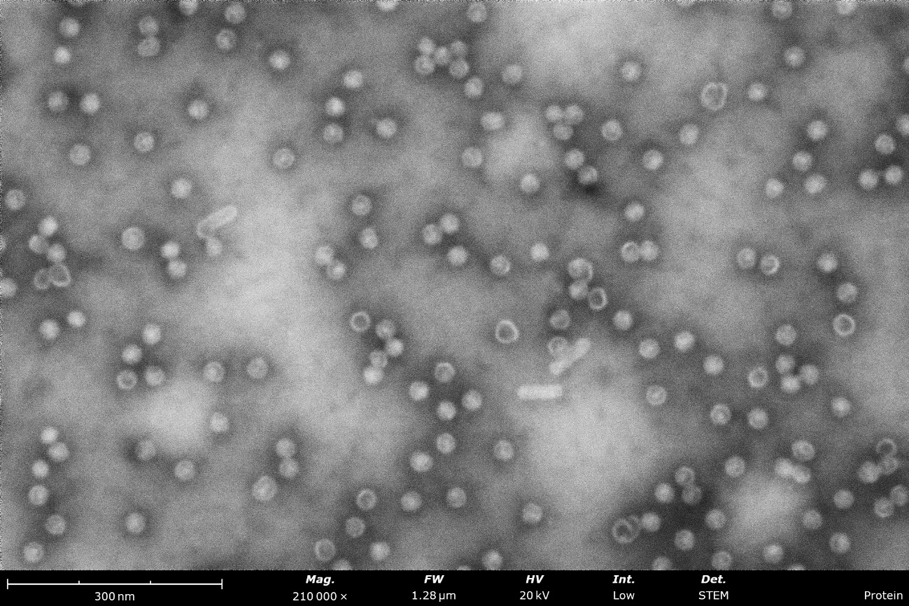
One of the primary reasons to consider purchasing a scanning electron microscope is its ability to provide unparalleled imaging resolution. Unlike traditional optical microscopes that rely on light waves to visualize samples, SEM employs a focused beam of electrons to achieve magnifications up to several hundred thousand times.
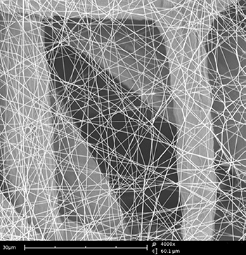
SEM images also provide a greater depth of field and enhanced contrast compared to optical microscopy. The choice to use a secondary electron detector (SED) or backscattered electron detector (BSD) provides researchers with the flexibility to tailor the image contrast to surface morphology or surface composition, respectively. This enables researchers to examine samples at an incredibly fine scale, revealing intricate surface details like sub-micron defects, thin layers, or interfaces. Such high-resolution imaging capabilities are crucial for fundamental research, quality control, and failure analysis in numerous industries.
2. Comprehensive Sample Analysis
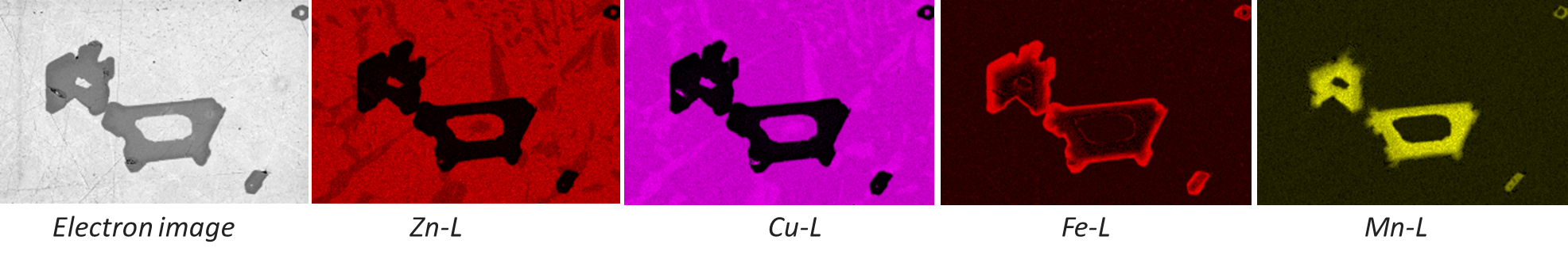
In addition to superior imaging resolution, SEMs offer a wide range of analytical techniques that allow for comprehensive sample analysis. These include energy-dispersive X-ray spectroscopy (EDS), electron backscatter diffraction (EBSD), and cathodoluminescence (CL).
EDS enables local elemental analysis and elemental mapping by detecting characteristic X-rays emitted from the sample that result from beam-sample interactions. An EDS detector, combined with dedicated software, is used to detect and process this data, discriminate between signal and noise, and perform quantitative analyses. Qualitative and quantitative EDS can provide valuable insights regarding the presence of trace elements and structure-processing relationships.
EBSD, on the other hand, can identify crystallographic information by collecting backscattered electrons using a specialized detector that preserves their spatial information. Integrated software is used to index the EBSD patterns allowing crystallographic phase and orientation to be visualized across a sample’s surface. This technique works best when the sample surface is polished and extremely smooth, which improves the sharpness of the EBSD pattern thereby improving signal-to-noise in the EBSD map. Ion milling is a proven technique for preparing high-quality surfaces for EBSD.
Cathodoluminescence (CL) is yet another multi-model technique that can be integrated into an SEM by adding a CL detector to the microscope column. The technique works by detecting the CL signal, which consists of visible light photons that are emitted from a sample’s surface when it is excited by the electron beam. Mapping the CL signal can be useful for identifying defective locations in semiconducting devices such as solar cells and light-emitting diodes (LEDs), exploring geological samples, and many other applications.

3. Three-dimensional (3D) Visualization
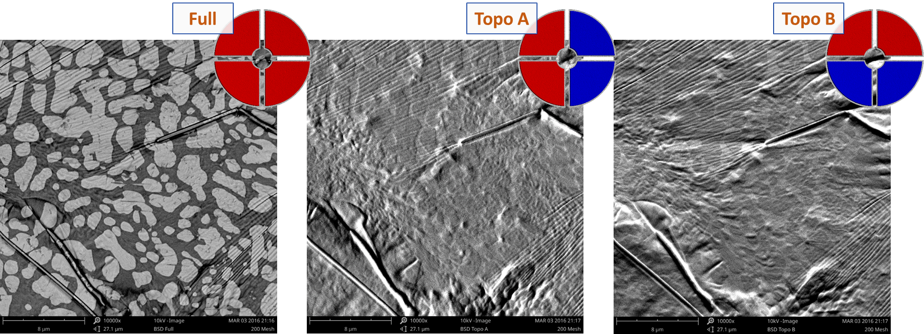
Another significant advantage of SEMs is their ability to generate three-dimensional visualizations of surface topography using orientation-dependent signals and shape-from-shading techniques. By using a segmented BSD, signals emanating from opposite sides of the sample can be detected at the same time and subtracted from one another to generate a qualitative surface topography image. This cancels out elemental contrast effects and exaggerates topographical contrast. More advanced image analysis software, such as the Phenom 3D Roughness Reconstruction Software can also be used to determine the average roughness (Ra) and roughness height (Rz).
4. Multi-disciplinary Applications
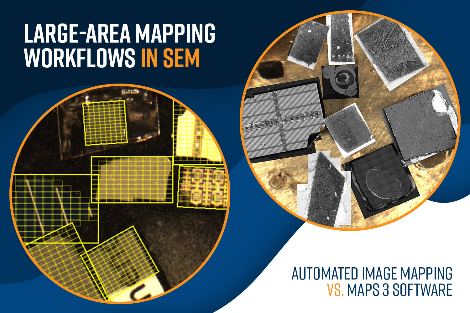
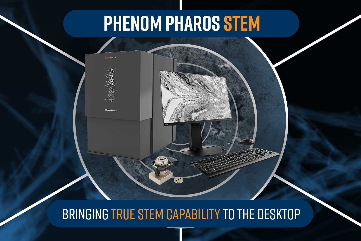
Scanning electron microscopes find applications in a diverse range of scientific disciplines and industries. Whether it is in biology, geology, nanotechnology, metallurgy, or forensics, SEM offers invaluable insights and analysis capabilities. Researchers can study cellular structures thanks to the improved resolution that scanning transmission electron microscopy (STEM) brings for samples thinned to the point of electron transparency. Materials that are susceptible to charging under the electron beam are clearly imaged through the use of low-kV and low-vacuum modes. With automation, standard workflows such as particle, fiber, or pore analyses can be made more efficient and free from human error, allowing scientists to make data-driven decisions faster.
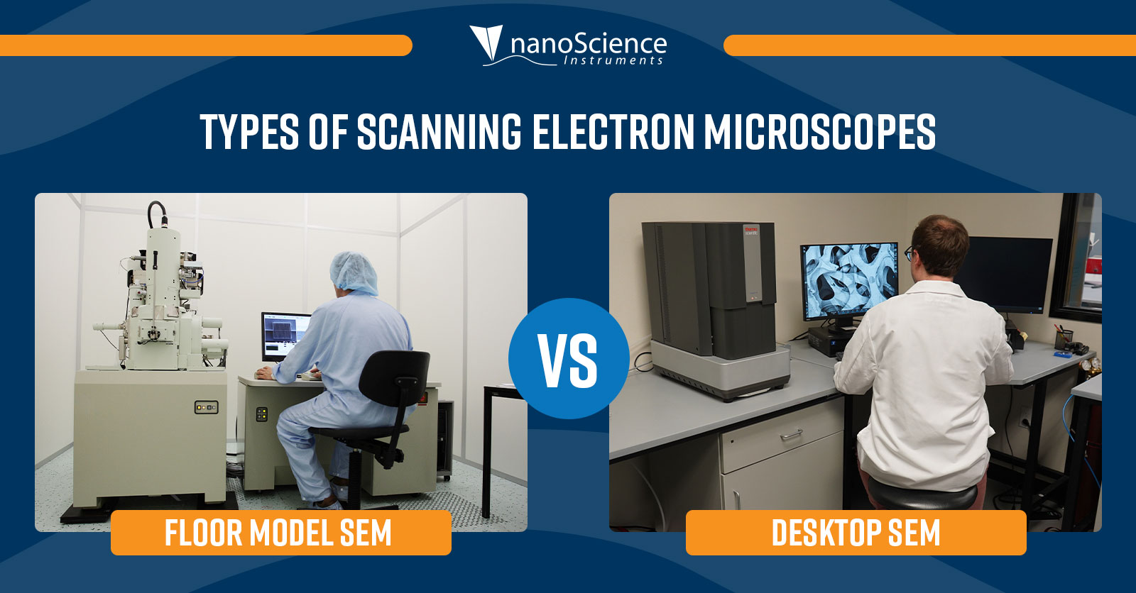
5. As a secondary instrument to increase productivity
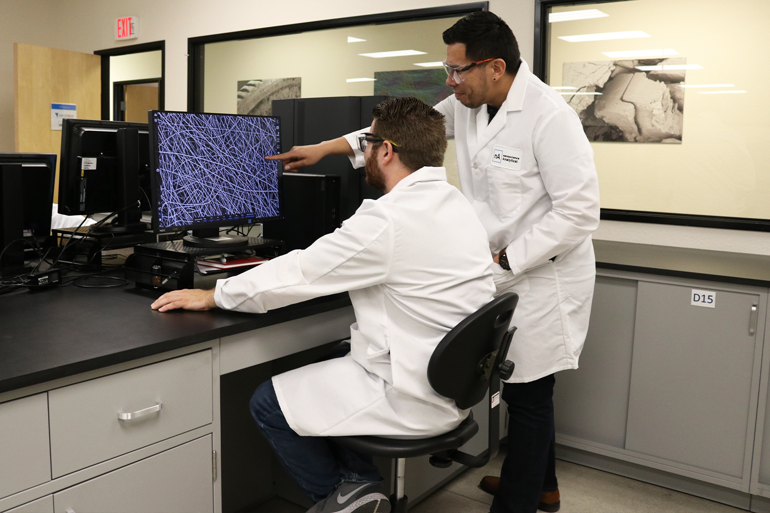
Owning multiple SEMs can provide several advantages in high-volume or R&D environments. In some cases, specific SEMs may be dedicated to a particular application. For example, one SEM may be equipped for performing automated particle analysis while a secondary SEM is optimized for low voltage imaging. Another common use case for a secondary SEM is that it may be used to screen samples before being analyzed in another SEM that is specialized for a certain task, such as milling of samples in the case of a dual-beam SEM. In these cases, the screening instrument helps to keep the workload on the specialized SEM more manageable by screening out samples that may not be good candidates for further data collection.
Having dedicated instruments enhances efficiency and ensures optimal performance for different applications. Like any complex instrument, SEMs can experience downtime due to maintenance, repairs, or unexpected issues. In time-sensitive environments, having the redundancy of a second SEM provides operational continuity when one SEM is temporarily unavailable.
Conclusion
Investing in an SEM can be a sensible decision for any organization or research institution seeking to delve deeper into the microscopic world. The exceptional imaging resolution, comprehensive sample analysis, three-dimensional visualization capabilities, and multi-disciplinary applications make SEM an indispensable tool for researchers and professionals alike. With its ability to reveal intricate details and unlock new insights, SEMs continue to push the boundaries of scientific discovery and technological advancements in countless fields.