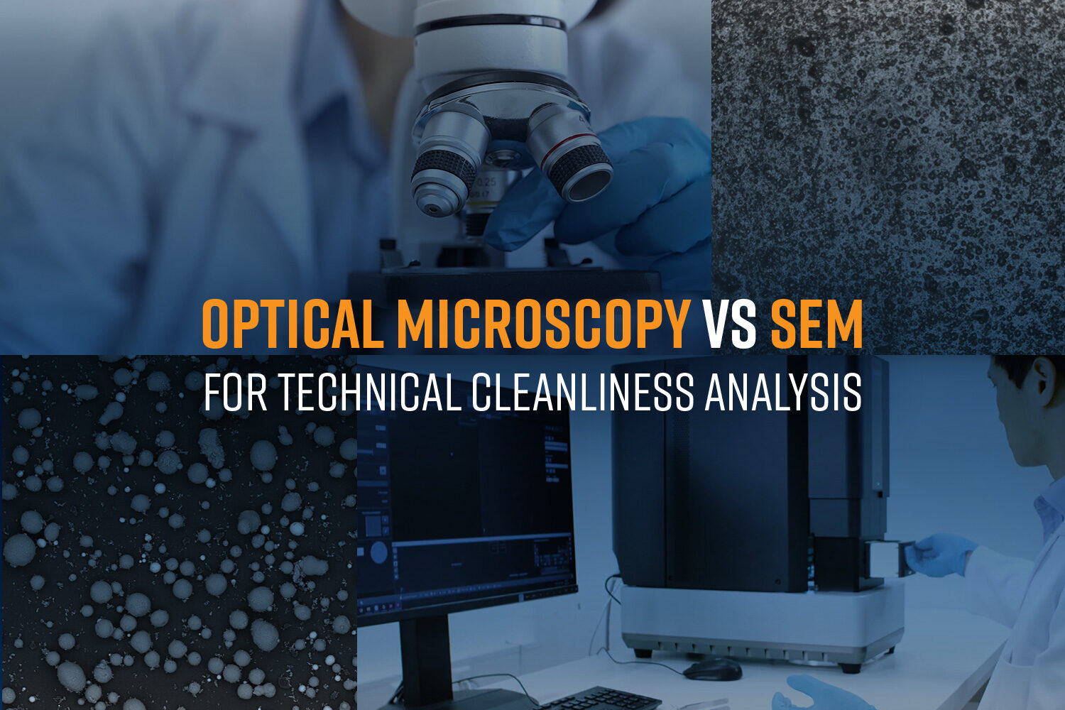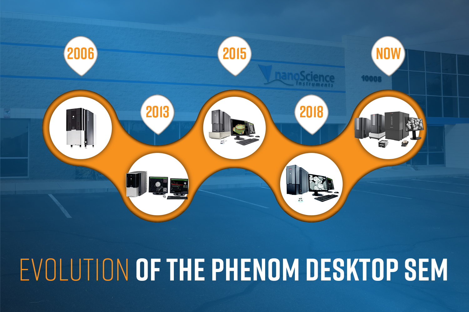
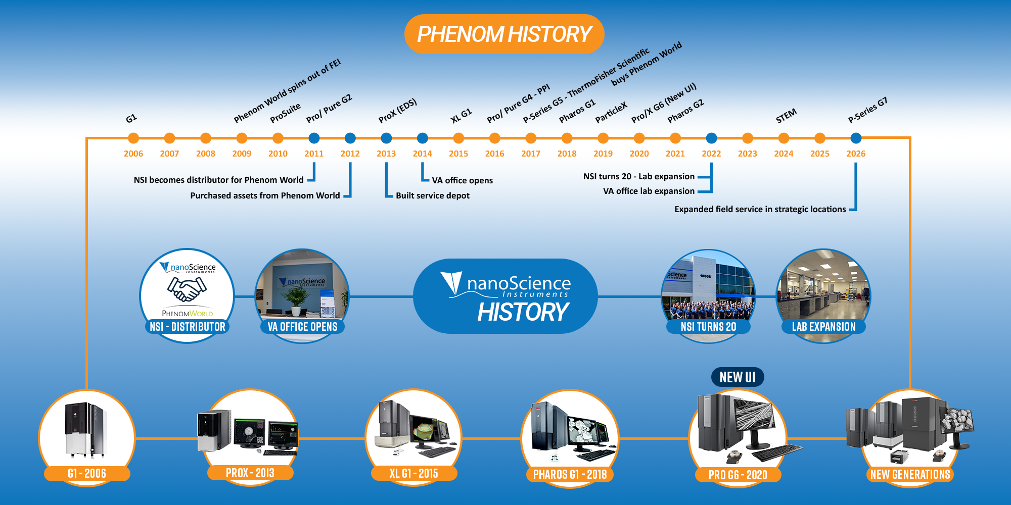
The Phenom Scanning Electron Microscope (SEM) is turning 20 this year! In celebration of this milestone, it is worth reflecting on how the platform has evolved, from the first true benchtop SEM bridging optical and electron microscopy, to a family of systems capable of advanced surface and transmission imaging, analysis, and automation. A condensed timeline for the Phenom and Nanoscience Instruments is shown in Figure 1.
Origins of Benchtop SEM Technology (2006-2009)
The introduction of the original Phenom desktop SEM in 2006 marked an important shift in electron microscopy. Developed by FEI Company, the system was designed to make SEM imaging faster, more accessible, and easier to use. With a resolution of 30 nm and magnification up to 20,000x, it filled a gap between optical microscopy and conventional SEM platforms.
Several hardware innovations defined the first generation of Phenoms:
- CeB6 electron source: Delivered significantly higher brightness and longer lifetime compared to tungsten sources, supporting more consistent imaging with reduced maintenance
- Differential pumping for specimen exchange: Enabled rapid sample loading and reduced contamination, allowing users to move from loading to imaging in under 60 seconds
- Navigation camera design: Provided an optical view aligned with the electron beam, improving sample targeting compared to traditional chamber cameras
- Integrated stage architecture: A mechanically stable design where the sample chamber locks directly to the electron column, enabling fast and repeatable positioning
- User-focused interface: Touch screen operation and an ergonomic control device (handheld knob) helped novice users gain confidence in SEM operation
In 2009, FEI Company spun out Phenom-World as a dedicated business entity to focus on advancing benchtop SEM technology specifically.

Workflow Improvements and Software Expansion (2010-2012)
With growing adoption of the first-generation Phenom SEM systems, the focus shifted toward usability and application-specific workflows. Phenom SEMs were commonly used as teaching tools, supporting nanotechnology education during this time. In 2010, Phenom-World introduced Phenom ProSuite, a software platform that significantly expanded instrument functionality for specific applications, capturing more attention from industrial companies and advanced laboratories. These tools (Figure 2) enabled users to move beyond simple imaging toward quantitative analysis.

Key capabilities of ProSuite:
- Automated image acquisition with stitching/tiling
- Remote SEM operation via a network interface
- 3D surface reconstruction and roughness analysis
- Fiber analysis (fiber diameter distribution, length, count, etc.)
In 2011, the 2nd Generation of Phenom instruments were released—the Phenom Pro G2 and Phenom Pure G2. The Phenom Pro G2 increased available magnification up to 45,000x while maintaining rapid time-to-image, and the Phenom Pure G2 provided a budget-conscious option for customers who needed an entry-level SEM. Detector option also expanded, allowing users to tailor imaging contrast for a wider range of materials.
During this period, early application-driven solutions like FiberMetric for fiber analysis in the nonwovens and textile industries demonstrated how the platform could be adapted to specific industry needs.
Analytical and Industrial Expansion (2013-2016)
The release of the Phenom ProX in 2013 marked a major transition from imaging to integrated analysis. With factory-integrated Elemental Identification (EID), the system incorporated energy dispersive x-ray spectroscopy (EDS/EDX) directly into the platform. This integration differentiated Phenom systems from its competitors, for which EDS was often a “bolt-on” third-party accessory. Users could now perform elemental mapping, line scans, and compositional analysis in an additional Phenom user interface window.
In 2015, the first-generation Phenom XL was introduced. This was the first of its kind, expanding the physical capabilities of benchtop SEMs by offering a sample stage with an area of 100 mm x 100 mm. Importantly, the larger stage did not affect the time-to-image, which remained under one minute. The Phenom XL allowed larger and more representative samples to be analyzed without sectioning, expanding the user base significantly. Automated stage movement enabled batch imaging of up to 36 standard 0.5” stubs and supported the new “single shot” navigation system. Users could click on an area of interest, then the stage would move that area under the electron beam for imaging and analysis.
By 2016, fourth-generation Phenom Pro and ProX systems introduced further column stability and even faster imaging performance. The introduction of the Phenom Programming Interface (PPI) further extended system flexibility, enabling automation and custom workflows through an open API.
Platform Integration and Industrial Automation (2017-2020)
In 2017, the Phenom Pro and ProX G5 systems were released, delivering a 20% improvement in resolution compared to the G4 systems. New software helped widen the Phenom’s application range, and a secondary electron detector (SED) became an option. Later that same year, Thermo Fisher Scientific acquired Phenom-World, bringing Phenom into a much broader ecosystem of detectors, software, and analytical tools.
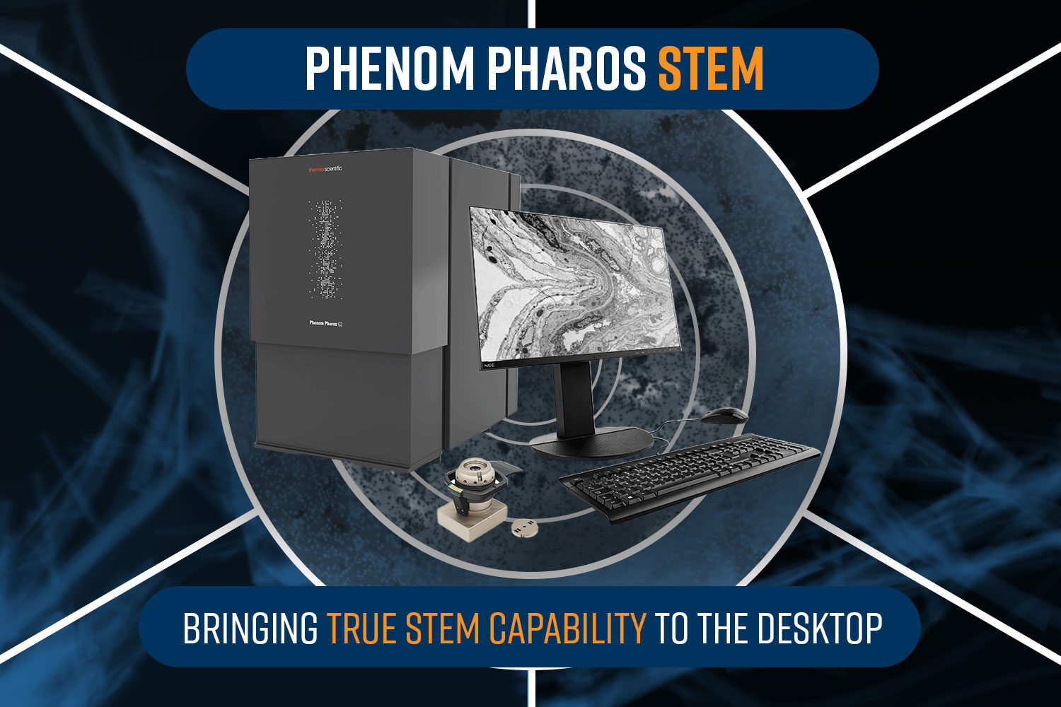
A major milestone came in 2018 with the introduction of the Phenom Pharos, the first and only benchtop SEM to use a field emission gun (FEG) electron source. This enabled sub-3 nm resolution, significantly higher beam coherence, and improved low-kV imaging for beam-sensitive materials such as polymers and coatings.
In 2019, the release of the ParticleX platform extended Phenom into fully automated industrial inspection. Designed for quality control environments, ParticleX enabled automated particle detection and classification, continuous unattended operation, and customizable reporting workflows based on industrial standards for forensic analysis, steel inclusion analysis, technical cleanliness, and more.
These developments supported the broader trend of decentralizing SEM access, moving systems out of core facilities and centralized laboratories, and closer to manufacturing and application environments.
Streamlined User Experience and Performance Gains (2020-2023)
The release of the Phenom Pro and ProX G6 systems in 2020 marked another step forward in performance, with resolution reaching 10 nm or better. At this stage, Phenom systems began to directly compete with some floor-model SEMs in terms of capability.
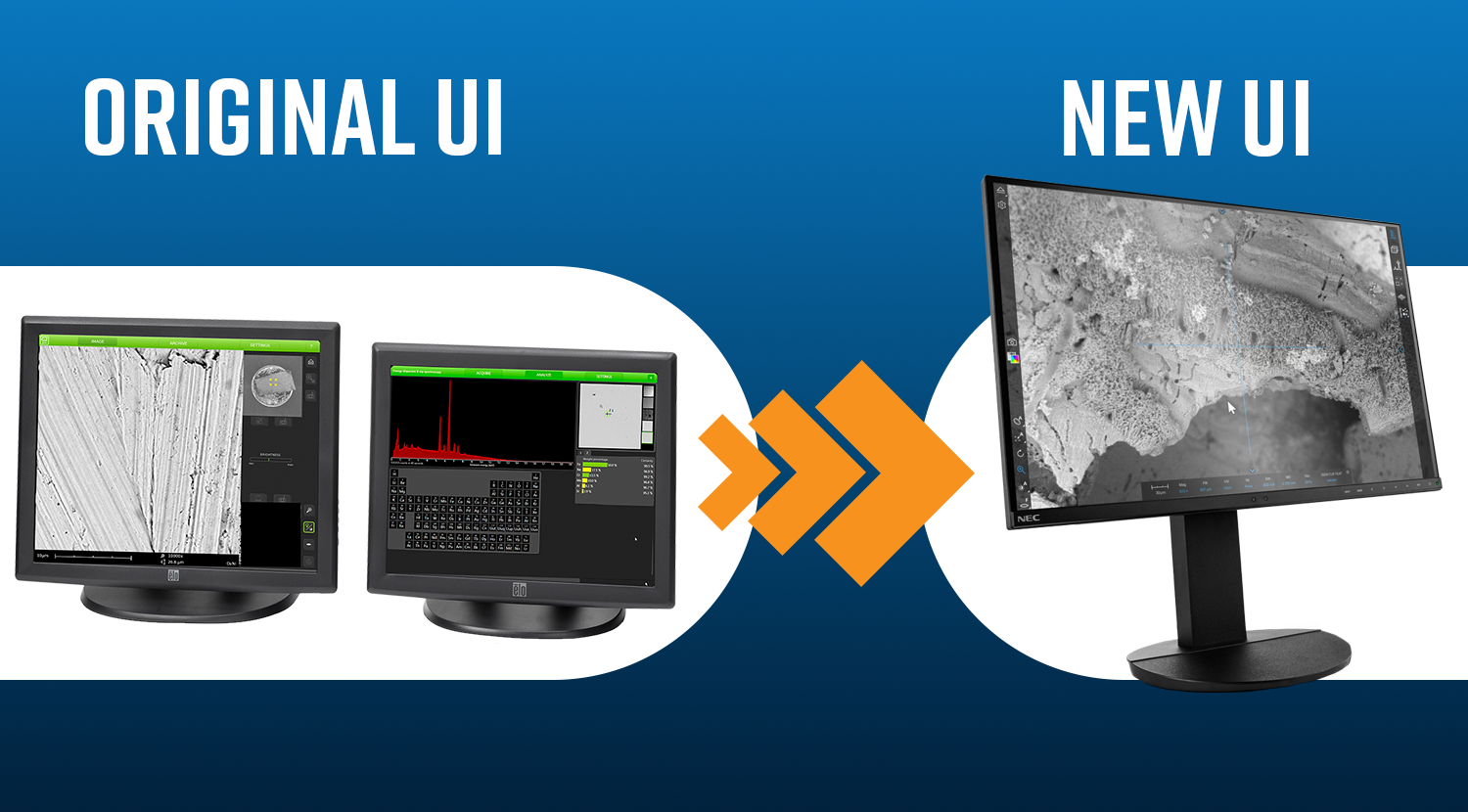
A redesigned user interface (UI) was a major part of the G6 launch, unifying imaging and analytical workflows into one widescreen UI shown in Figure 3. This new UI environment simplified transitions between SEM imaging and EDS or application software like FiberMetric, ParticleMetric, and others, eliminating the need for a second monitor.
In 2021, the Phenom Pharos G2 further improved the Pharos’ popular FEG performance, achieving sub-2 nm resolution and extending magnification capabilities to 2,000,000x.
This era also marked a shift away from the original Linux-based Phenom operating system toward a more standardized software environment, aligning with modern IT requirements and enabling better integration across the Thermo Fisher ecosystem.
Correlative Workflows & Expanded Analytical Platform (2024-2025)
Recent developments have focused on expanding analytical flexibility, improving industry-specific workflows, and enabling more automated operation across the Phenom platform.
In 2024, a STEM detector/sample holder was introduced for the Phenom Pharos G2, enabling true transmission imaging within a benchtop SEM. The Phenom STEM holder has multiple independently addressable detector segments, each corresponding to a defined electron scattering angle range. By selecting or combining these segments, users can configure imaging modes such as Bright Field (BF), Dark Field (DF), and High-Angle Annular Dark Field (HAADF), or application-specific custom modes. It can also still be used for traditional SEM imaging and EDS to evaluate surface features by switching to SEM mode. This further extends the platform into applications that traditionally required costly Transmission Electron Microscopes (TEMs) such as nanomaterial analysis, grid screening for cryo-EM, tissue ultrastructure imaging, and other advanced applications.
In parallel, software innovation has played a major role in expanding the capabilities of Phenom systems in the past few years:
- MAPS for Phenom enabled fully automated large-area imaging, multi-modal dataset stitching, and cross-instrument correlation, supporting standardized workflows across microscopy techniques
- ChemiSEM introduced real-time, quantitative elemental mapping directly within the SEM workflow. This allows users to visualize composition live during imaging rather than relying on post-processing
- ChemiPhase built on ChemiSEM by enabling phase identification and quantification through advanced statistical analysis of SEM-EDS datasets. This allows users to distinguish chemically distinct phases and report their relative abundance, supporting applications such as alloy characterization and multiphase materials analysis
- Python-based automation tools and the continued evolution of the Phenom Programming Interface (PPI) allow users to develop fully customized workflows, enabling deeper integration into laboratory and industrial processes. It has also played a significant role in the development of “self-driving” or “autonomous” materials science labs.
- Avizo Trueput extended analysis into high-throughput, AI-driven workflows, particularly for complex materials datasets where automated segmentation and quantification are critical
Together, these software advancements reflect a broader shift in the Phenom platform, from a fast, accessible imaging tool to a fully integrated analytical powerhouse capable of handling increasingly complex industrial materials characterization challenges.
Looking Ahead (2026 and On)
In 2026, Thermo Fisher Scientific released the 7th generation Phenom Pure, Pro, and ProX systems. The new generation introduced improvements in electron optics, detector performance, and automation workflows, further enhancing image quality and analytical capabilities while maintaining the rapid time-to-image and ease-of-use that define the Phenom family of instruments. Resolution improved, along with better low-kV performance for challenging and beam-sensitive materials. The G7 platform also delivered faster elemental mapping and more streamlined automated workflows for industrial and research applications. Additionally, the redesigned hardware of the G7 systems increased the lifetime of the CeB6 source by 100%, guaranteeing 3,000 hours of performance compared to the previous specification of 1,500 hours.
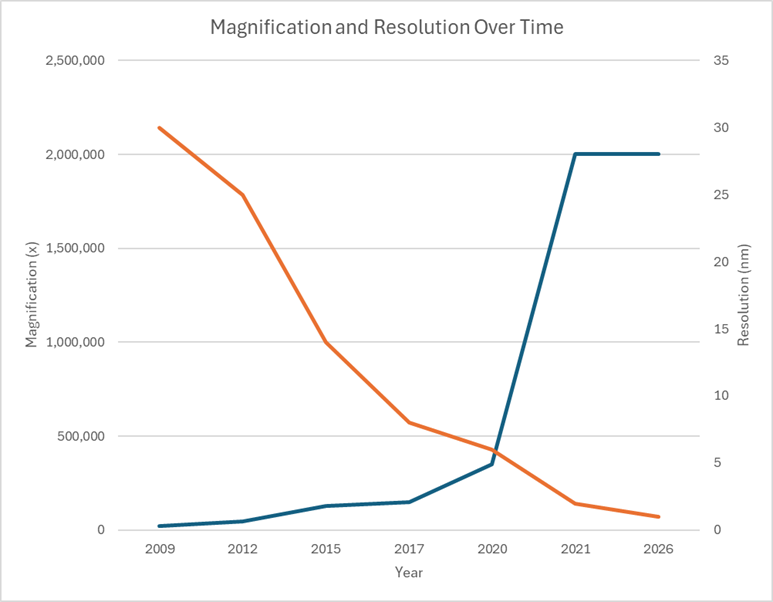
Over the past two decades, the Phenom platform has maintained a consistent focus on accessibility, speed, and exceptional image quality. These improvements are demonstrated by the graph in Figure 4, which plots resolution and magnification against time. Early innovations in source technology, vacuum column design, and sample handling established a strong hardware foundation, while ongoing developments in software and automation capabilities have expanded the Phenom’s role across research and industry. As applications continue to evolve, from materials science to industrial quality control and increasingly, life sciences, the Phenom Desktop SEM remains positioned as a flexible yet powerful solution for modern microscopy labs.
Nanoscience Instruments & Phenom
Since its inception in 2002, Nanoscience Instruments has played a significant role in the adoption and support of Phenom desktop SEM technology across the United States, with more than 1,300 systems installed in academic, industrial, and government laboratories. The company’s relationship with the Phenom platform dates back to the early stages of its commercialization, when benchtop SEM technology was still emerging as a viable alternative to conventional electron microscopy.
In 2011, Nanoscience Instruments became the exclusive North American distribution partner for Phenom-World, establishing a direct channel between the manufacturer and end users. This partnership enabled a localized approach to customer engagement, including application-focused technical sales, method development, and hands-on training. As Phenom systems expanded beyond basic imaging into analytical and application-specific workflows, this close collaboration ensured that users had access not only to the instrumentation itself, but also to the expertise required to implement it effectively in real-world environments.
At the end of 2012, Nanoscience Instruments purchased the assets of Phenom-World North America, including the service depot and existing maintenance contracts. Over the next year, Nanoscience Instruments built out their own formal service facility for Phenom SEMs at its headquarters in Phoenix, Arizona, where a specialized team of Phenom-World-certified engineers began providing both in-house repairs and nationwide field service. In 2014, Nanoscience Instruments expanded its footprint with the opening of an East Coast office and laboratory in Alexandria, Virginia, enabling faster response times and more accessible support for Phenom customers across the eastern United States. This expanded service infrastructure significantly reduced instrument downtime while strengthening the feedback loop between customers, service engineers, and the broader Phenom development teams.
Over time, Nanoscience Instruments has also contributed to the expansion of Phenom applications by working closely with customers across diverse industries, including materials science, pharmaceuticals, electronics, energy, aerospace, automotives, and industrial manufacturing. These collaborations have helped translate emerging analytical needs into practical workflows, particularly in areas such as particle characterization, failure analysis, fiber and textile analysis, and automated quality control, among many others.
Today, the Nanoscience Instruments Phenom support team includes a dedicated group of electron microscopy specialists focused on application development, a growing team of service engineers, and technical sales team members strategically located across the country. The applications team supports method development, training, and advanced workflow implementation. The service engineers provide on-site maintenance and services in customers’ labs, and in parallel, the Phoenix service depot continues to serve as a central hub for instrument maintenance, refurbishment, upgrades, and complex repairs.
This combination of local expertise, service infrastructure, and long-standing collaboration with the Phenom platform has positioned Nanoscience Instruments as a key contributor to the continued growth and evolution of benchtop SEM technology in North America.