Enhancing Efficacy of Bipolar Membranes through Electrospinning
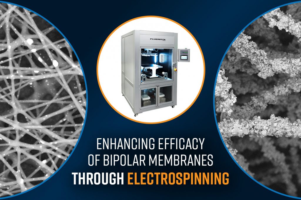
Electrospinning has emerged as a transformative technique for fabricating fibrous materials with highly controlled geometries. This method, characterized by its ability to produce ultrafine fibers from various materials, has garnered widespread attention across industries, including healthcare, energy, and materials science. A particularly exciting aspect of electrospinning is its capacity to create complex geometric structures composed of nanoscale and microscale fibers, which significantly enhance their functionality for advanced applications. Traditional electrospinning produces planar surfaces composed of randomly oriented fibers but advancements in the field have enabled the fabrication of more sophisticated structures. In this blog we will delve into some of the complex geometric structures that can be fabricated by electrospinning and their different applications.
Microscopy & Microanalysis 2025 | July 28 – July 31, 2025 | Salt Lake City, Utah
Join us in Salt Lake City, Utah for the highlight of the microscopy calendar – M&M 2025! Nanoscience Instruments is back for this annual summertime conference, and this time we’re showcasing in Booth #1925.
Evaluating Alternative Techniques for Real-Time Monitoring of Molecular Interactions at Surfaces
Understanding molecular interactions at surfaces is essential for advancing fields such as biosensing, materials science, and drug discovery. These interactions—ranging from protein-ligand binding to polymer adsorption—can reveal crucial information about binding kinetics, affinity, and conformational changes. Surface-sensitive analytical techniques enable researchers to monitor these events in real time and under physiologically relevant conditions, without the […]
ACS Colloids 2025 | June 22-26, 2025 | Edmonton, AB
99th ACS Colloids & Surface Science Symposium Mark your calendars for the 99th ACS Colloid and Surface Science Symposium! The event promises to be an unparalleled gathering of researchers, scholars, and professionals from around the world, focusing on the cutting-edge advancements in the field of colloid and surface science. Visit us at table #B4 to […]
Nanoscience Instruments Becomes Exclusive North American Distributor for SenseAI
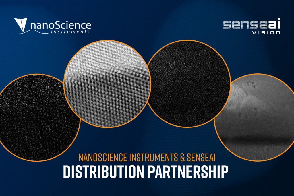
Nanoscience Instruments will be the sole North American sales and service provider of electron microscopy imaging software SenseAI Vision. Liverpool, UK – May 1st 2025 SenseAI, the compressed sensing software transforming the way electron microscopy images are captured, is excited to announce a new exclusive distribution agreement with Nanoscience Instruments, leaders in microscopy and surface […]
2-Day QCM-D Short Course | Alexandria, VA | September 2025
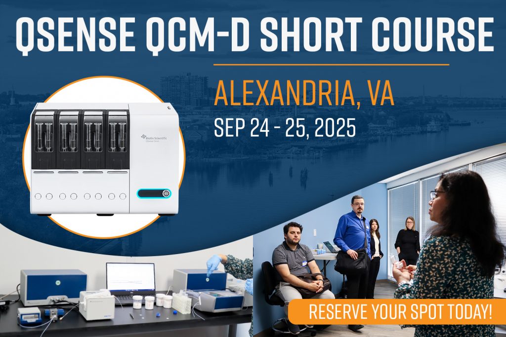
2-Day QCM-D Short Courses: Join our specialized 2-day QCM-D (Quartz-crystal Microbalance with Dissipation monitoring) Short Course. Held in Alexandria, VA, this immersive program is designed for both experienced practitioners and newcomers, offering an in-depth exploration of both fundamental and advanced QCM-D techniques. Hosted at our state-of-the-art facilities, the course features hands-on sessions with the latest […]
2-Day SEM Short Course | Phoenix, AZ | November 2025

2-Day SEM Short Courses: Explore the microscopic world in our specialized 2-day Scanning Electron Microscopy (SEM) Short Course. Held in Phoenix, AZ during the fall, this immersive program is designed for both experienced practitioners and newcomers, offering an in-depth exploration of both fundamental and advanced SEM techniques. Hosted at our state-of-the-art facilities, the course features […]
Nanoscience & Xplore Instruments Announce Strategic Partnership for Distribution of Polymer Micro Compounding Equipment
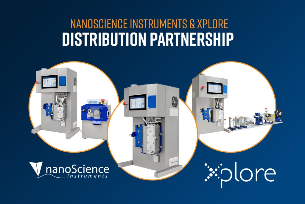
Nanoscience Instruments and Xplore Instruments BV Announce Strategic Partnership for Distribution of Polymer Micro Compounding Equipment in the US New collaboration enhances accessibility to advanced polymer processing solutions in North America Nanoscience Instruments, a leading provider of scientific instrumentation and service solutions for customers in the United States and Canada, is excited to announce a […]
Maximizing Efficiency in Polymer R & D with Microcompounders
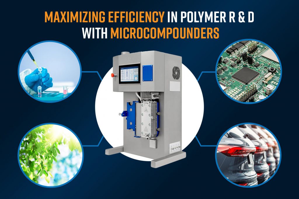
In polymer processing and material research, achieving uniform dispersion and distribution of additives and precise formulation control is crucial for developing advanced materials. This is achieved by a process called compounding. Microcompounding Microcompounding is a small-scale polymer processing technique that involves mixing, blending, and modifying polymer materials using a specialized miniaturized instrument. It mimics […]
Desktop Scanning Electron Microscopy in Geology
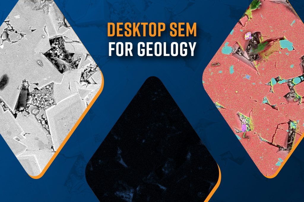
Scanning Electron Microscopy (SEM) is a versatile tool in geology used in high-resolution imaging and chemical analysis of rocks, minerals, and microfossils. SEM provides detailed images of mineral morphology and surface textures, which are essential for identifying minerals and understanding their growth patterns. Studying the deformation features using an SEM helps reconstruct the geological history […]