2-Day QCM-D Short Course | Alexandria, VA | Feb. 2026
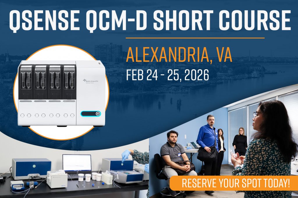
2-Day QCM-D Short Courses: Join our specialized 2-day QCM-D (Quartz-crystal Microbalance with Dissipation monitoring) Short Course. Held in Alexandria, VA, this immersive program is designed for both experienced practitioners and newcomers, offering an in-depth exploration of both fundamental and advanced QCM-D techniques. Hosted at our state-of-the-art facilities, the course features hands-on sessions with the latest […]
What are the Key Applications of QCM-D?
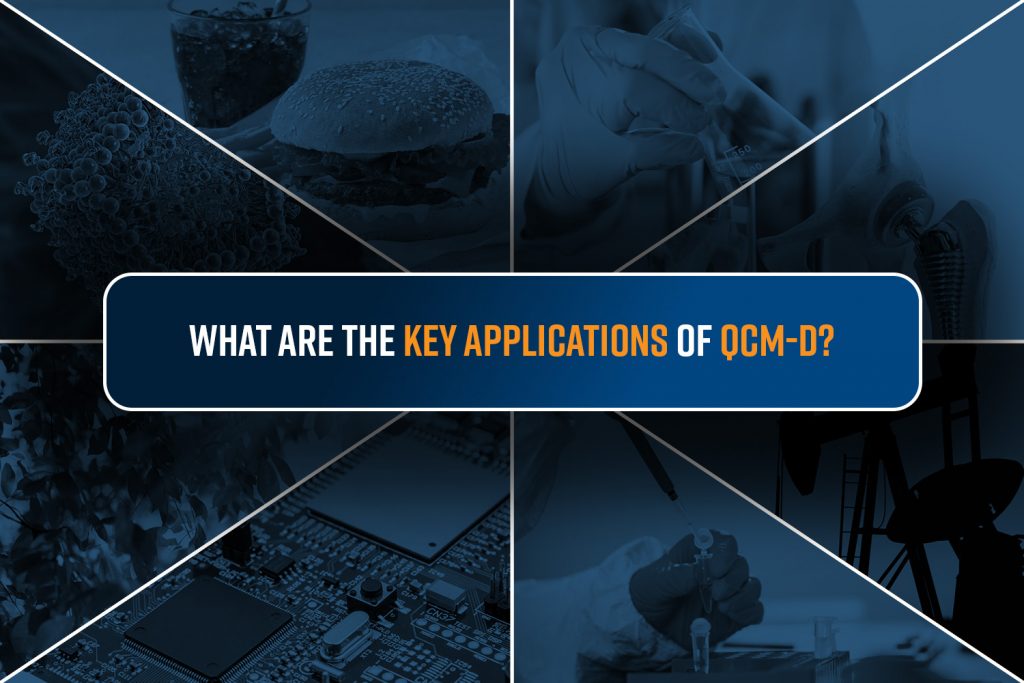
Quartz Crystal Microbalance with Dissipation monitoring (QCM-D) has revolutionized surface science by enabling real-time analysis of molecular interactions. However, traditional QCM-D workflows often involve time-consuming manual processes that introduce variability and inefficiency. In most QCM-D systems, sensor mounting, determining the resonance frequencies, stabilizing the baseline in air, priming the sensor, and establishing the baseline in liquids are performed manually.
A Guide to Particle Analysis: Key Methods, Applications, and Benefits
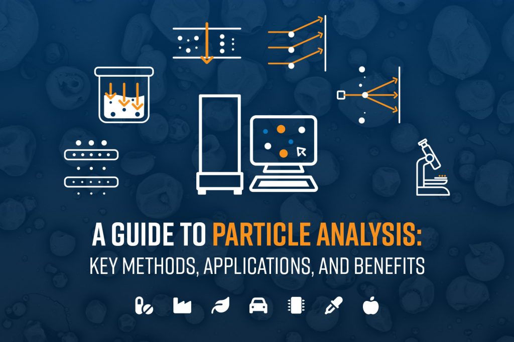
What is Particle Analysis? Particle analysis is the measurement and characterization of particles in a sample. Particle analysis typically focuses on properties such as particle size and size distribution, shape and morphology, count, concentration, and composition. Particle analysis is used to ensure quality control, understand material properties, and optimize production processes. Techniques for Particle Analysis: […]
Desktop SEMs: Advanced Imaging Without the Infrastructure
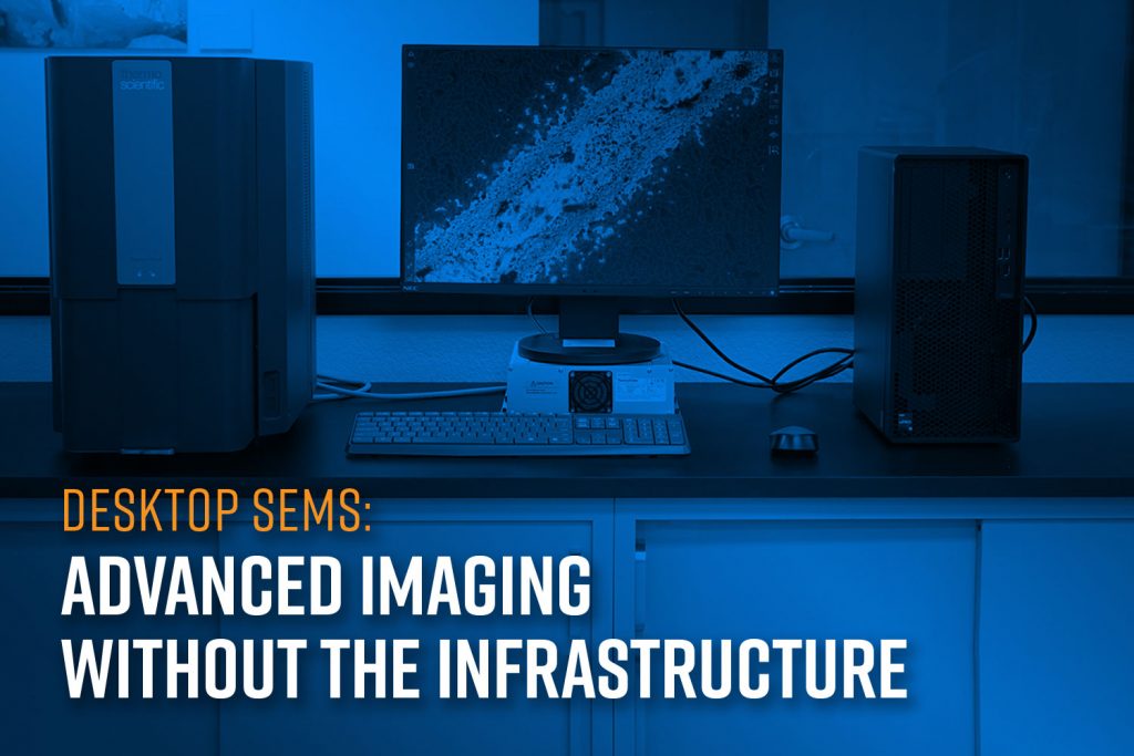
Scanning Electron Microscopes (SEMs) are indispensable tools for analyzing surface morphology, materials composition, and microstructural details at high resolution. They are used extensively across research institutions, manufacturing lines, forensic labs, environmental monitoring stations, and more. However, conventional floor-model SEMs come with significant infrastructure requirements, such as dedicated space, environmental conditioning, and auxiliary systems, that often […]
2025 NanoNews: SEM Edition Q2
We’re pleased to share the latest edition of nanoNews! In the second quarter of the 2025 newsletter, you’ll find our webinar resources, event news, and our newest articles and technical notes – all focused on Scanning Electron Microscopy (SEM).
2025 NanoNews: QCM-D Edition Q2
Welcome to the Quartz Crystal Microbalance with Dissipation monitoring (QCM-D) edition of the Nanoscience Instruments newsletter, nanoNews. We are excited to share the latest updates from around the QCM-D community with you!
2025 NanoNews: Electrospinning Edition Q2
2025 NanoNews: Tensiometry Edition Q2
Welcome to the second quarter Tensiometry edition of the Nanoscience Instruments newsletter, nanoNews. We are excited to share the latest updates from around the Tensiometry community with you!
Fabricating Nanofibers: Electrospinning Vs Blow Spinning
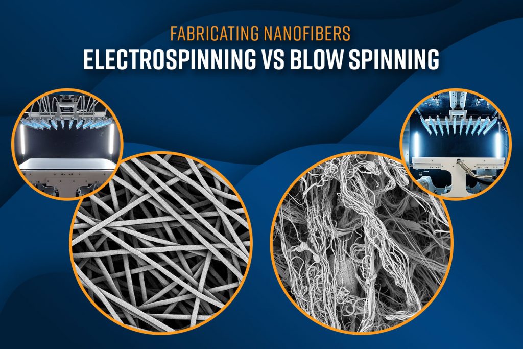
Nanofibers, with their high surface area-to-volume ratio, tunable porosity, and mechanical flexibility, are increasingly used in diverse applications including filtration, biomedical devices, energy storage, and smart textiles. Among the many fabrication techniques available, electrospinning and blow spinning have emerged as two of the most prominent methods for producing nanofibers from polymeric solutions. While both techniques can yield continuous nanofibers, they differ significantly in their operational principles, equipment requirements, scalability, fiber morphology, and suitability for different applications.
American Chemical Society (ACS) Fall 2025 | August 18-20, 2025 | Washington, DC

ACS Fall 2025 Meet us in Booth #2719 at the American Chemical Society’s Fall Meeting! Stop by for a live electrospinning demo with the Fluidnatek LE-50 G2, our compact and powerful benchtop unit. We will also have a QSense Omni and an Attension Theta Flow for hands-on exploration of the instruments and their powerful software! […]