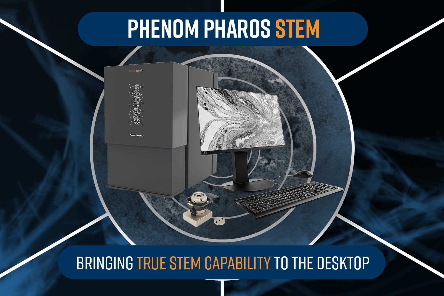
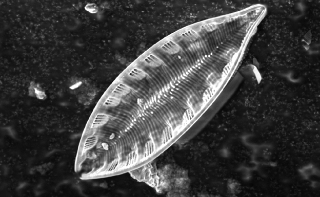
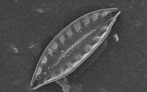
The fundamental unit of electric charge is the electron, an elementary particle that can be used in the domain of microscopy to see beyond the diffraction limit of optical light and uncover the microscale characteristics of many different types of materials. A scanning electron microscope (SEM) is an analytical tool that creates highly magnified images by raster scanning the surface of a sample with a beam of electrons and processing the various signals produced by atomic interactions. Because formation of the image depends on localized electron signals, charge buildup can be detrimental to the resulting image quality, resulting in beam drift, uneven brightness, and blurred regions on the image.
The nature of electric charge buildup
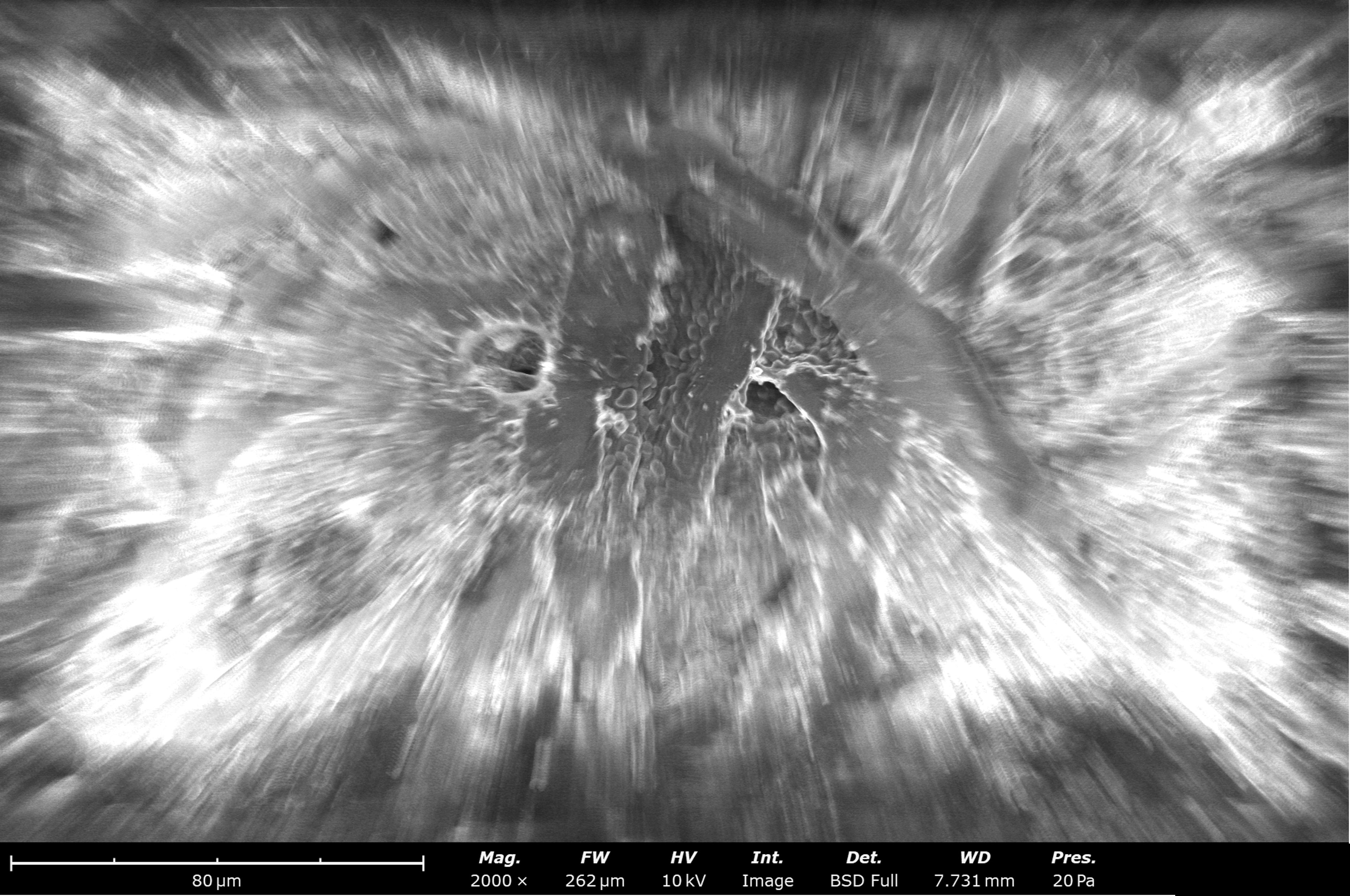
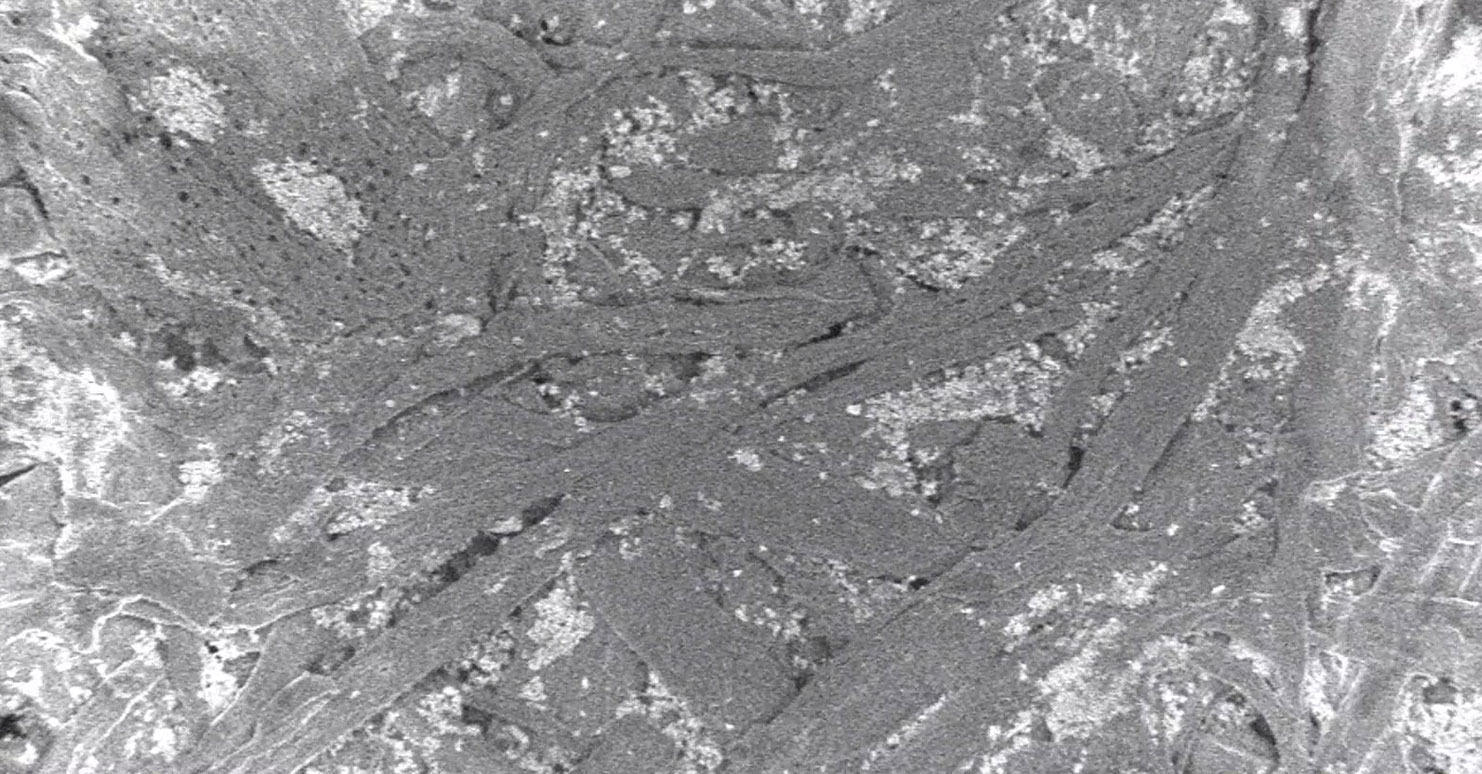
Atoms are hindered from conducting electrons in electrically insulating materials. As such, it can be difficult to dissipate the accumulated charge to ground without additional workarounds. As negative charge accumulates on the surface of samples, an abundance of signal is detected, causing image artifacts such as “glowing” bright areas that expand with time. Another consequence of overcharging is beam drift – the phenomenon wherein the image blurs and appears to move. Imaging non-conductive samples can be achieved not only with a conductive coating layer, but with variable pressure and low kV e-beam settings as well.

The principle of balancing charge
When a sample is struck with an electron beam, there are a few possible outcomes that affect the total charge at the sample surface:
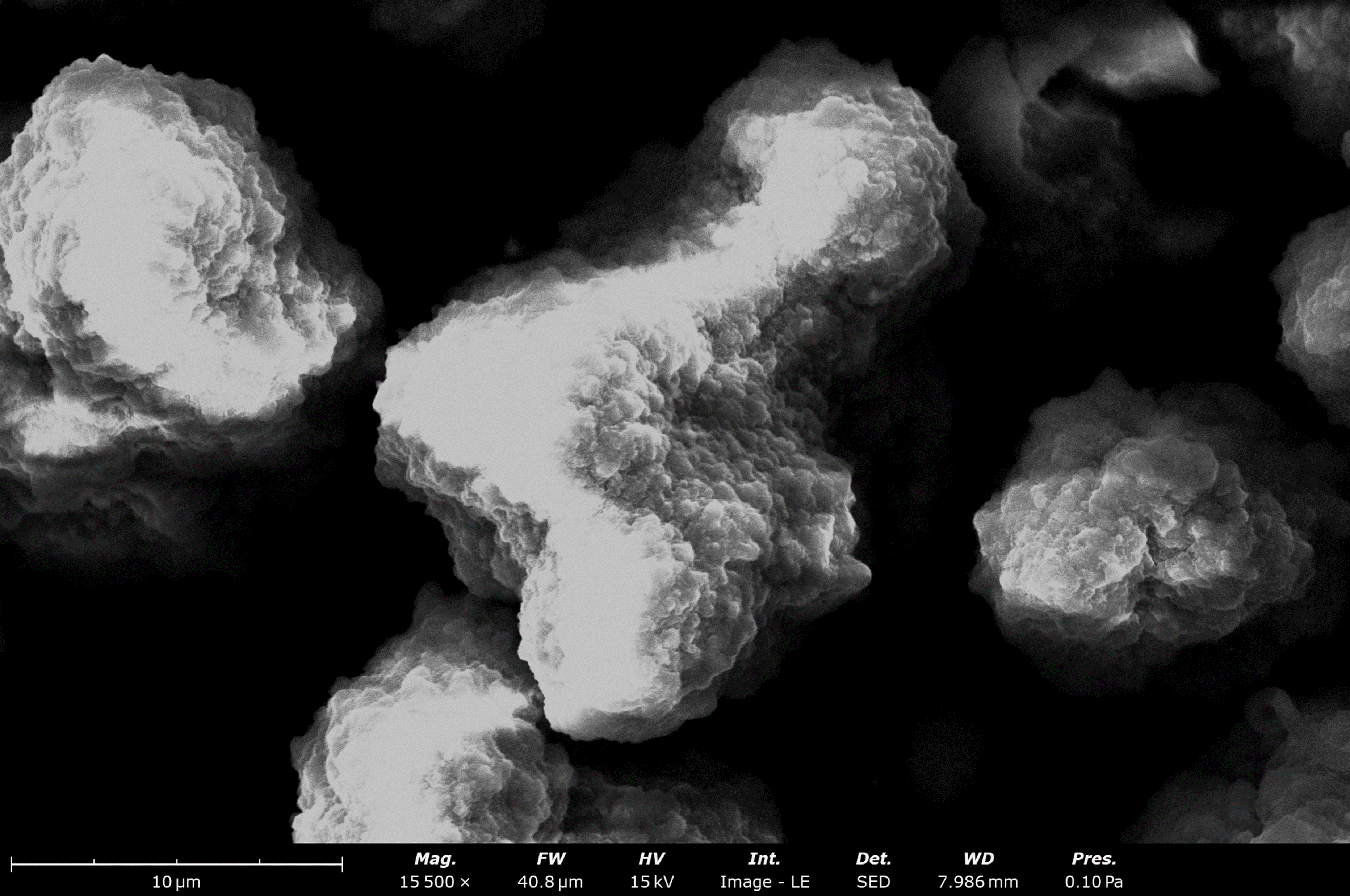
- Negative charging – occurs when incident electrons are trapped within the sample, causing glowing bright regions due to excess signal
- Positive charging – occurs when the rate of electron emission is greater than the beam current provides, causing dark regions due to the lack of signal
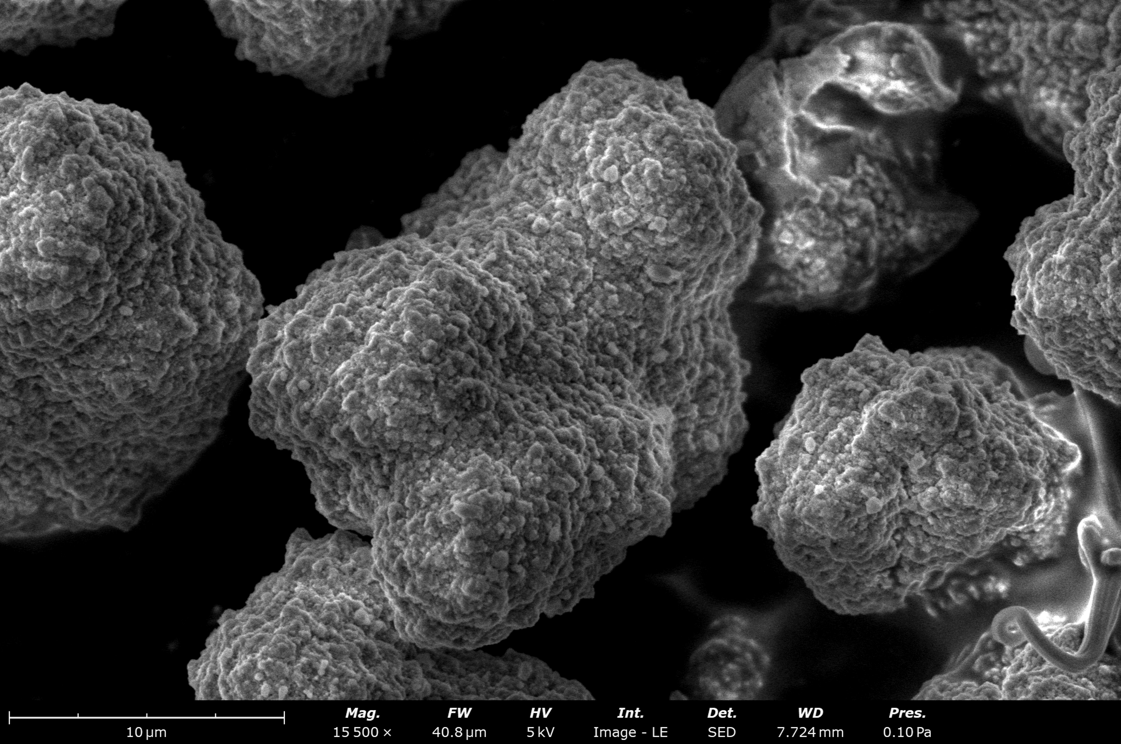
- Neutrality – the primary electrons absorbed by the sample are conducted to ground, and leaves the local surface charge unchanged, resulting in no image artifacts
How to combat charging
Low voltage imaging: turn down accelerating voltage
Accelerating voltage – quantified in kilovolts (kV) – is the parameter that controls the energy the electrons gain over the difference in potential supplied by the electron gun. With high kinetic energy, electrons will travel at great speeds and penetrate deeply into the surface of the sample, thereby lessening the likelihood of their escape. Lower accelerating voltages mitigate this electric charge buildup on the surface by increasing the share of both backscattered electrons and secondary electrons emitted from the sample. Electrons from the beam arriving with less kinetic energy are unlikely to be embedded deep into the surface, providing a useful strategy of preserving a more neutral net charge.
Every non-conducting material has a unique accelerating voltage where charge balance can be achieved. This experimentally determined value depends on the sample composition, structure, thickness, and roughness as well as the beam energy and current. In general, accelerating voltages between 2 and 5 kV have been found to be successful in reducing charging artifacts.
Sputter coating with conductive material
Sputter coating is the process of depositing a thin layer of conductive metal grains onto the surface of a sample to provide a pathway for excess electrons to ground. The most common material used in sputter coating is gold, though platinum, carbon, and palladium are commonly employed in many sputter coating devices as well. One of the downsides of sputter coating becomes apparent in the case of energy dispersive X-ray spectroscopy measurements or imaging using the BSE detector: elemental-based signals will be biased to the coating material. Metal coatings also increase the secondary electron emission from the surface, making it a great option for topographical analysis. However, surface characteristics may be slightly altered or more difficult to detect depending on the coating thickness.
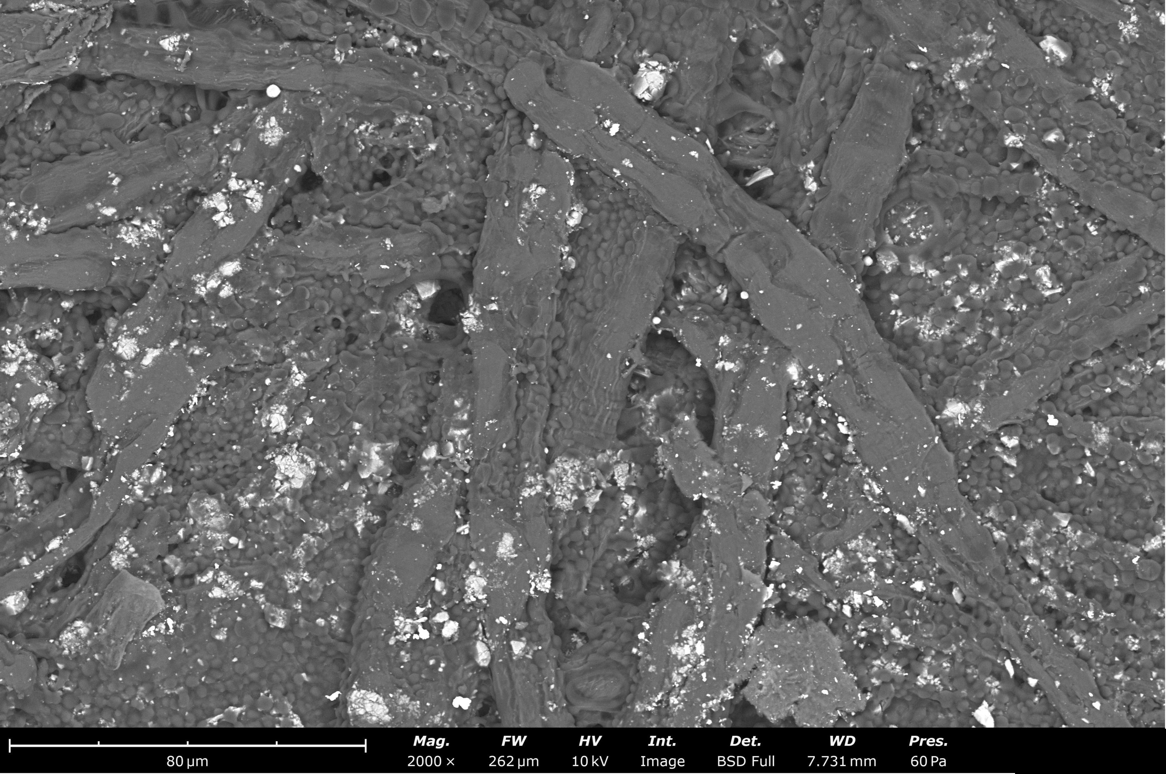
Low vacuum imaging
Low vacuum imaging is a method which introduces a gas, usually air or water vapor, inside the sample chamber to collect electrons and discharge them on a grounded surface within. An overabundance of gas molecules can disrupt the electron beam itself, so the number of molecules must be controlled to maintain the low vacuum environment. Isolating the column vacuum from the sample chamber is key to achieving control, but this also creates a limitation: many SEMs are not equipped with the technology to implement low vacuum imaging. Furthermore, traditional secondary electron detectors are unable to work in low vacuum conditions. Therefore, low vacuum imaging sacrifices a significant degree of topographical information because only the BSE signal may be collected. It is a great option for non-conductive samples that cannot be sputter coated and may be used in combination with low voltage imaging for particularly challenging analyses.