The Battery Show South 2025 | April 16-17, 2025 | Atlanta, GA
Nanoscience Instruments provides solutions for battery development applications through cutting-edge instrumentation and analytical services. Visit our booth for live demonstrations of desktop SEM with automated workflows designed for structural and chemical analysis of battery materials, and learn about our surface characterization tools, battery cyclers & potentiostats, and process development and analytical services.
Fabricating Complex Geometries with Electrospinning
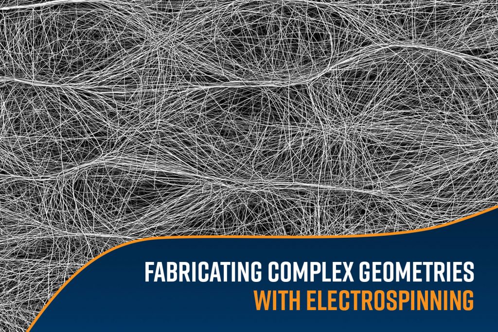
Electrospinning has emerged as a transformative technique for fabricating fibrous materials with highly controlled geometries. This method, characterized by its ability to produce ultrafine fibers from various materials, has garnered widespread attention across industries, including healthcare, energy, and materials science. A particularly exciting aspect of electrospinning is its capacity to create complex geometric structures composed of nanoscale and microscale fibers, which significantly enhance their functionality for advanced applications. Traditional electrospinning produces planar surfaces composed of randomly oriented fibers but advancements in the field have enabled the fabrication of more sophisticated structures. In this blog we will delve into some of the complex geometric structures that can be fabricated by electrospinning and their different applications.
5 Benefits of Scanning Electron Microscopy for Particle Analysis

Particle analysis is a critical process in many industries, from pharmaceutical formulation and nanomaterials development to forensic investigations and industrial manufacturing. Understanding the size, shape, and composition of particles plays a crucial role in ensuring product quality, optimizing performance, and meeting regulatory requirements.
Unmatched Sensitivity: How QSense Omni Redefines QCM-D Performance
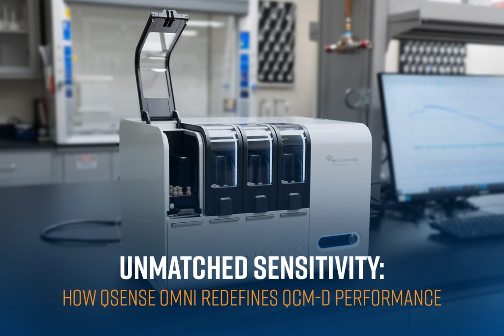
Interactions at surfaces and interfaces are crucial in many fields, including environmental science, biopharmaceutical research, materials science, catalysis, and nanotechnology. The ability to detect minute changes in mass, viscoelastic properties, and interfacial phenomena can be crucial in determining the success of groundbreaking research. Understanding these interactions allows for the design of better materials and devices with tailored properties.
American Chemical Society (ACS) Spring 2025 | March 24 – 26, 2025 | San Diego, CA

ACS – American Chemical Society Meet us in Booth #3625 at the American Chemical Society’s Spring Meeting! In the meantime, we invite you to explore our wide range of solutions and services for chemists, including: Nanomaterial Fabrication Systems Nanomaterial Characterization Tools Process Development & Analytical Services To learn more about the capabilities of our dedicated Analytical […]
Particle Analysis Techniques: What Makes SEM Unique

Particle analysis involves measuring various characteristics of powders or particulates, including size, shape, and composition. A wide variety of industries rely on particle analysis for ensuring product functionality and safety including the production of automobiles, batteries, pharmaceuticals, and electronics.
Electrospinning: A Versatile Technique for Fabricating Diverse Fiber Microstructures
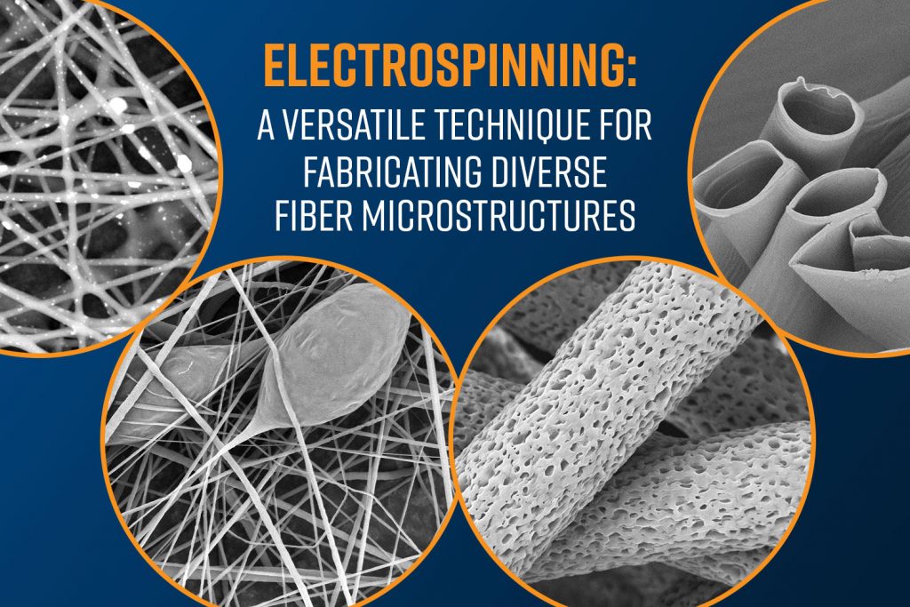
Electrospinning is a powerful and versatile technique used to produce nonwoven ultrafine fibers with controlled microstructures. Electrospinning can be used to fabricate fibers of different diameters ranging from 20 nm to more than 10 µm. Fibers can be fabricated from solution, emulsion, suspension, sol-gel or slurry composed from different materials like polymers (natural, semi-synthetic and synthetic), ceramics, metals and/or different types of additives. Its ability to process a wide range of materials and produce fibers with tailored properties has made it a cornerstone in applications like textiles, medical & healthcare, energy, filtration, packaging, automotive, and aerospace.
Large-area Mapping Workflows in Scanning Electron Microscopy (SEM)
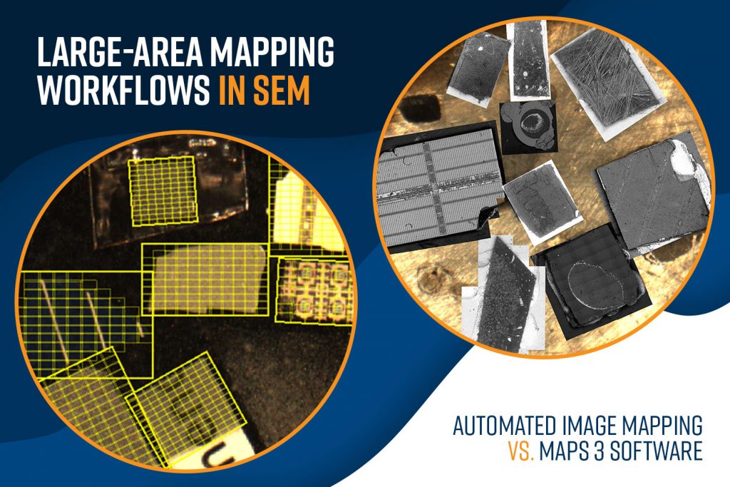
Large-area imaging in scanning electron microscopy (SEM) is a technique for exploring expansive regions of a sample at high resolution, making it invaluable in fields such as materials science, electronics, and life sciences. However, capturing high-resolution images across large sample areas presents unique challenges, including time constraints and data management. This is where image stitching algorithms come into play, enabling researchers to seamlessly combine multiple high-magnification images into a single, comprehensive view (often referred to as a large-area map). In this blog, we’ll dive into how large-area mapping works, explore various image stitching software and workflows, and discuss how these techniques can improve efficiency and enhance imaging results.
2-Day SEM Short Course | Alexandria, VA | May 2025
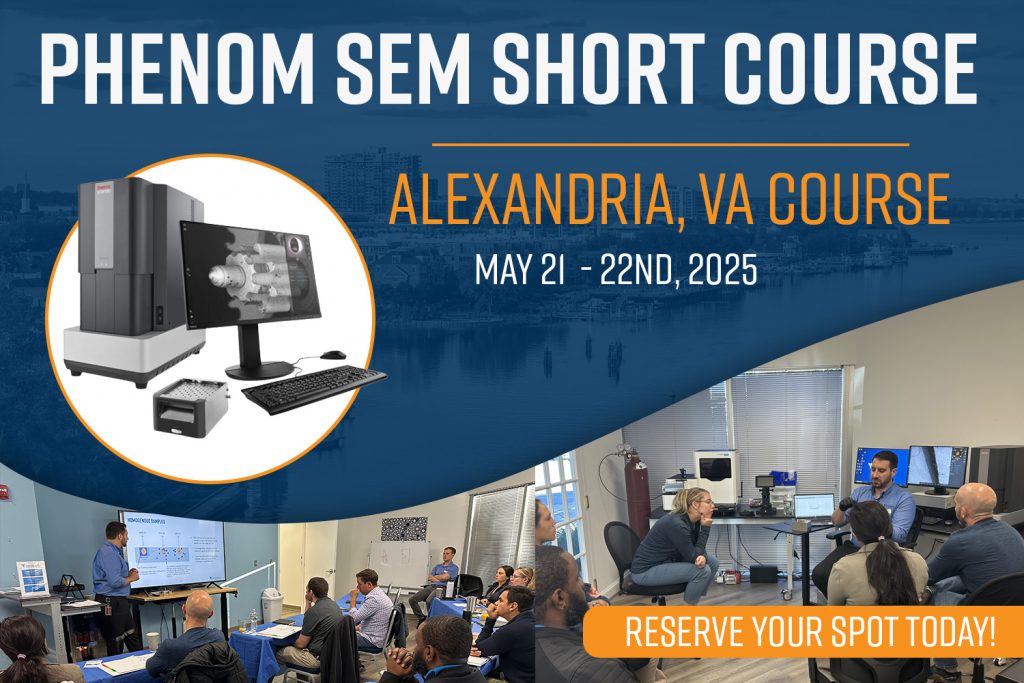
2-Day SEM Short Courses: Explore the microscopic world in our specialized 2-day Scanning Electron Microscopy (SEM) Short Course. Held in Alexandria, VA, this immersive program is designed for both experienced practitioners and newcomers, offering an in-depth exploration of both fundamental and advanced SEM techniques. Hosted at our state-of-the-art facilities, the course features hands-on sessions with […]
Medical Design & Manufacturing West 2025 | Feb. 4-6, 2025 | Anaheim, CA

MD&M West – Medical Design & Manufacturing West Nanoscience Instruments and our sister company, Nanoscience Analytical, provide cutting-edge instrumentation and process development services to enhance the production of medical devices and biomedical products such as tissue scaffolds, vascular grafts, wound healing therapeutics, and more. Visit us in Booth #541 to learn about the power and […]