The electron source is one of the most important components of a scanning electron microscope (SEM) and is a major factor in determining its maximum analytical performance. There are three common types of electron sources found in SEMs: tungsten filaments, solid state hexaboride crystals, and field emission guns.
How do electron sources work?
As the name suggests, the electron source is the component responsible for generating a beam of high-energy electrons in the SEM. Commonly referred to as an electron gun, the source must be able to emit a bright and stable stream of electrons for consistent focusing on the sample. This beam raster scans across a field of view (around tens to hundreds of micrometers) to generate a high-magnification image of the sample surface.
The most common type of electron source used in SEM is a thermionic emitter, with tungsten wire filaments and solid-state hexaboride crystals – made of cerium hexaboride (CeB6) or lanthanum hexaboride (LaB6) –falling into this category. Thermionic emission for SEMs is the process in which electrons are released from a material by resistive heating with a current. Once the energy provided by heat surpasses the work function of the surface, electrons are emitted in great abundance (~109/s).
Field emission guns are the second class of electron sources used in SEM. Field emission guns function through the quantum phenomenon of tunneling to extract electrons from the gun material. An electric field is applied to an extremely sharp metal tip (usually fabricated from a single crystal of tungsten) which leads to very coherent and bright electron emission.
So, which type of electron source is better? The short answer is it depends. In general, you’ll need to consider your unique application and specimen, analytical performance requirements, and budget when choosing the appropriate electron source.
Tungsten filament
The tungsten hairpin was the source used for the first generation of electron microscopes and remains the most common source used to this day. Tungsten sources are relatively cheap, designed to be replaced quickly and easily during regular usage of the SEM.
While they are the lowest cost option, tungsten emitters also provide the least performance compared to the other electron sources. The theoretical resolution of tungsten hairpins is worse than LaB6 crystals or FEGs due to the significantly larger emission area of the hairpin (Table 1).
| Tungsten hairpin | CeB6 crystal | Schottky FEG | |
|---|---|---|---|
| Emission mechanism | Thermionic | Thermionic | Electron Tunnelling |
| Lifetime | 100 h | 1500 h | >10,000 h |
| Tip emitting diameter | 100 µm | 25 µm | 100 nm |
| Resolution @30 kV | 4 nm | 3 nm | 1 nm |
| Resolution @1 kV | 50 nm | 25 nm | 5 nm |
| Low-kV imaging (<5 kV) | Yes | No | Yes |
| Vacuum | 10-1 – 10-5 mbar | 10-7 mbar | 10-9 mbar |
| Cost of ownership | Lowest | Medium | Highest |
Table 1: Comparison of electron source characteristics for SEM.
Tungsten thermionic sources operate at white-hot temperatures, around 2800 K, causing them to evaporate over time and risk contaminating the column and sample. This also makes the source prone to sudden burnout during imaging sessions, which can pose significant disruptions especially when it happens during sensitive sample analysis. The average lifetime of a tungsten hairpin source is about 100 beam-on hours. These sources also undergo thermal cycling every time the column is vented for sample exchange causing frequent changes to the beam stigmation and alignment. This results in blurry SEM images, and must be manually corrected by users throughout the imaging session.
LaB6 / CeB6 crystal
These sources utilize a highly polished crystal of lanthanum hexaboride (LaB6) or cerium hexaboride (CeB6) for thermionic emission. Hexaboride crystals have a lower work function than Tungsten, allowing them to emit ten times as many electrons as Tungsten across all accelerating voltages. The brighter beam provides two key advantages: higher signal-to-noise and higher resolution, making them a popular choice for most SEM applications.
They are significantly more stable than tungsten, and always remain warm and under vacuum, so they require much less tuning and last about 10 to 15 times longer before requiring replacement. The source lifetime slowly degrades over time and doesn’t suddenly burn-out, meaning that replacements can be planned in between sessions.
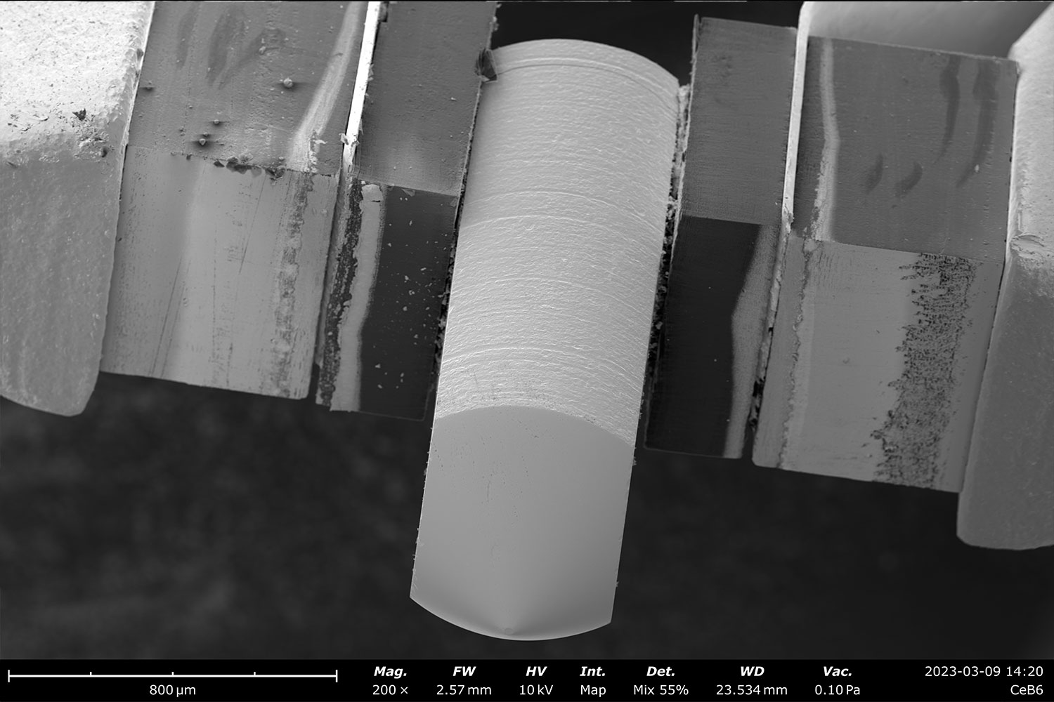
Hexaboride based electron guns only require stigmation adjustments every 3-6 months, rather than the continuous adjustments common with tungsten-based SEMs. While both LaB6 and CeB6 materials provide similar performance, the newer CeB6 sources have become more common in recent years thanks to their better resistance to evaporation and thereby better longevity. These sources, however, do require higher vacuum levels than tungsten hairpin sources (see Table 1) and temperature control to ensure they operate properly.

Field Emission Gun (FEG)
FEG sources contain an extremely fine tip fabricated from a single crystal of tungsten and rely on electron tunneling to emit electrons. SEMs typically utilize a Schottky FEG, which functions as a field-assisted thermionic emitter. This allows it to emit the brightest and most coherent beam of electrons making it excellent for applications requiring high spatial resolution.
Studying thin film coatings, nanoparticles, or nano-scale features that could be missed while using a CeB6 source are just a few applications where FEG-based SEMs excel in. Operating at low accelerating voltages (<5 kV) with a FEG-equipped SEM makes it possible to get quality data from beam-sensitive materials and insulators without the use of a conductive coating.
FEG electron sources require the highest vacuum levels but also come with the longest operation lifetimes. Similar to the hexaboride sources, replacement time can be reliably predicted, and catastrophic burnout does not occur. Although the costliest option of electron sources, they deliver superior performance in every application.