
Electrospinning is a voltage-driven material fabrication process that can be used to produce micro to nano-scale fibers. The electrospinning process is a combination of interacting…
Posted: August 9, 2023 | Technology: Electrospinning & Electrospraying

An optical tensiometer, also known as a contact angle goniometer, is an instrument used to characterize material surface properties and interactions between liquid and solid…
Posted: August 3, 2023 | Technology: Tensiometry
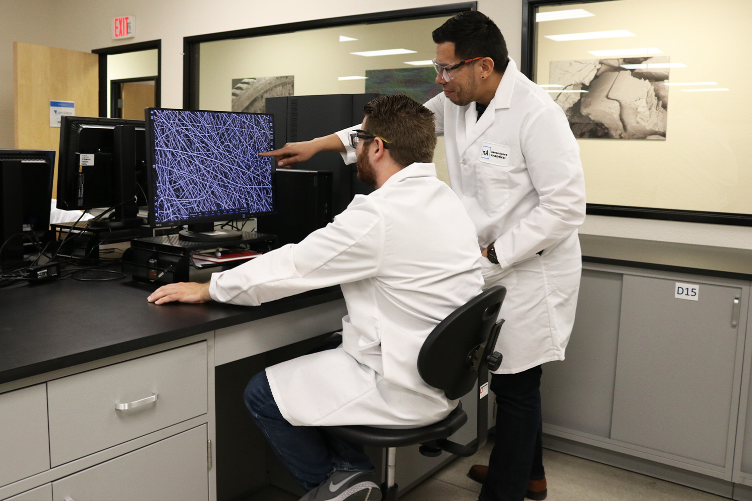
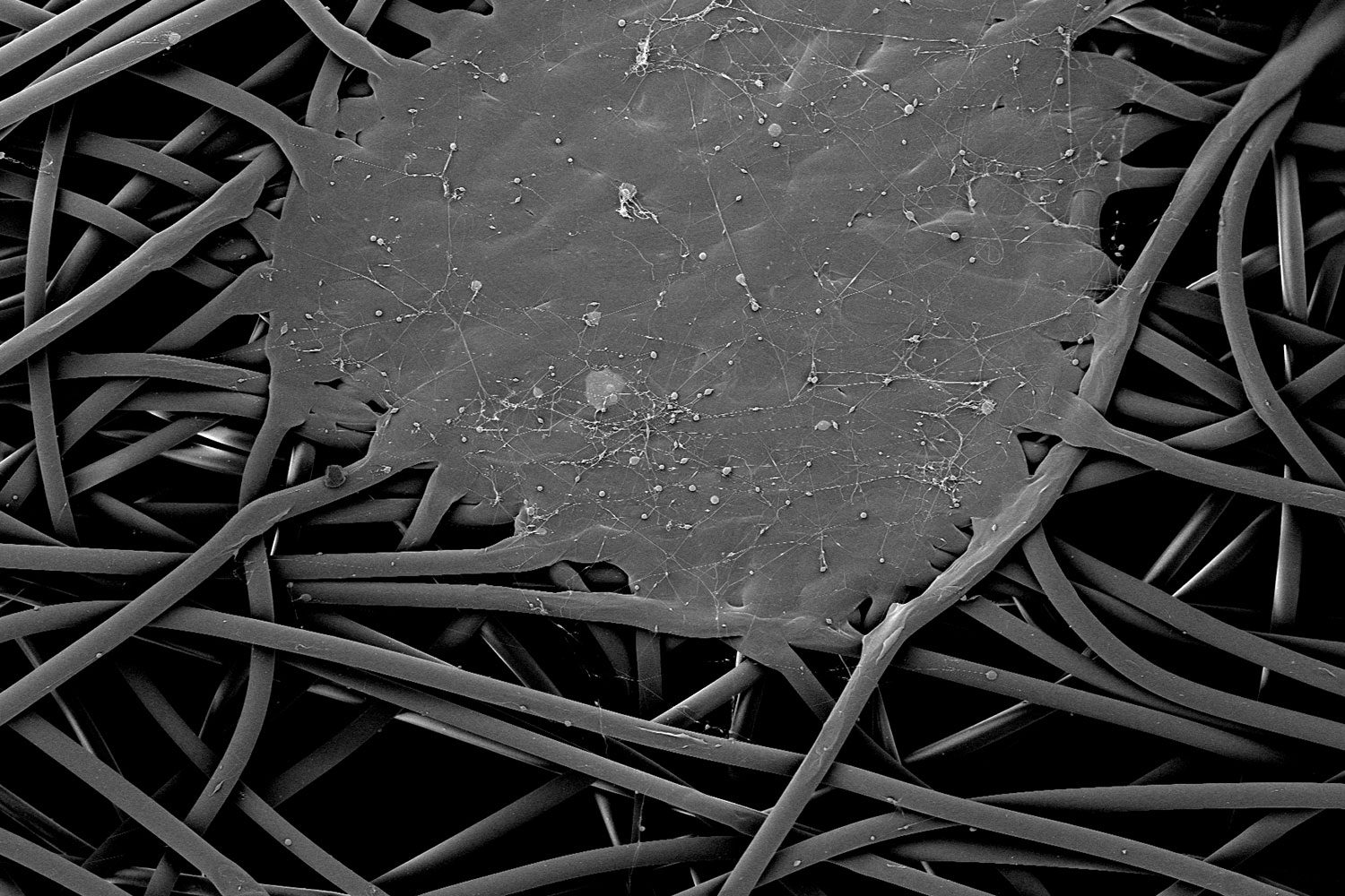
Scanning electron microscopy (SEM) is a technique that employs a focused beam of electrons to scan a surface, point by point, to examine a sample’s…
Posted: July 19, 2023 | Technology: Scanning Electron Microscopy
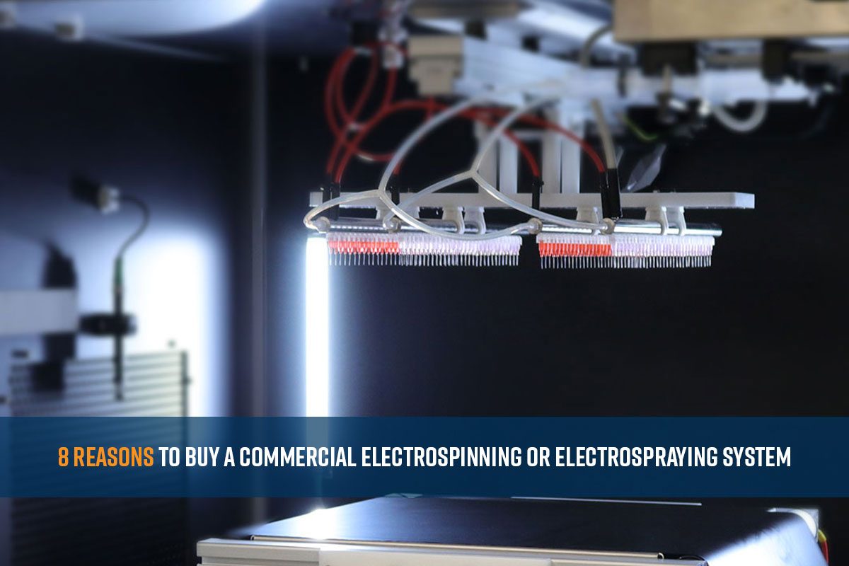
Electrospinning and electrospraying are electrohydrodynamic processes wherein a polymer solution is used to fabricate fibers or particles, respectively. In the most basic setup, a polymer…
Posted: July 17, 2023 | Technology: Electrospinning & Electrospraying
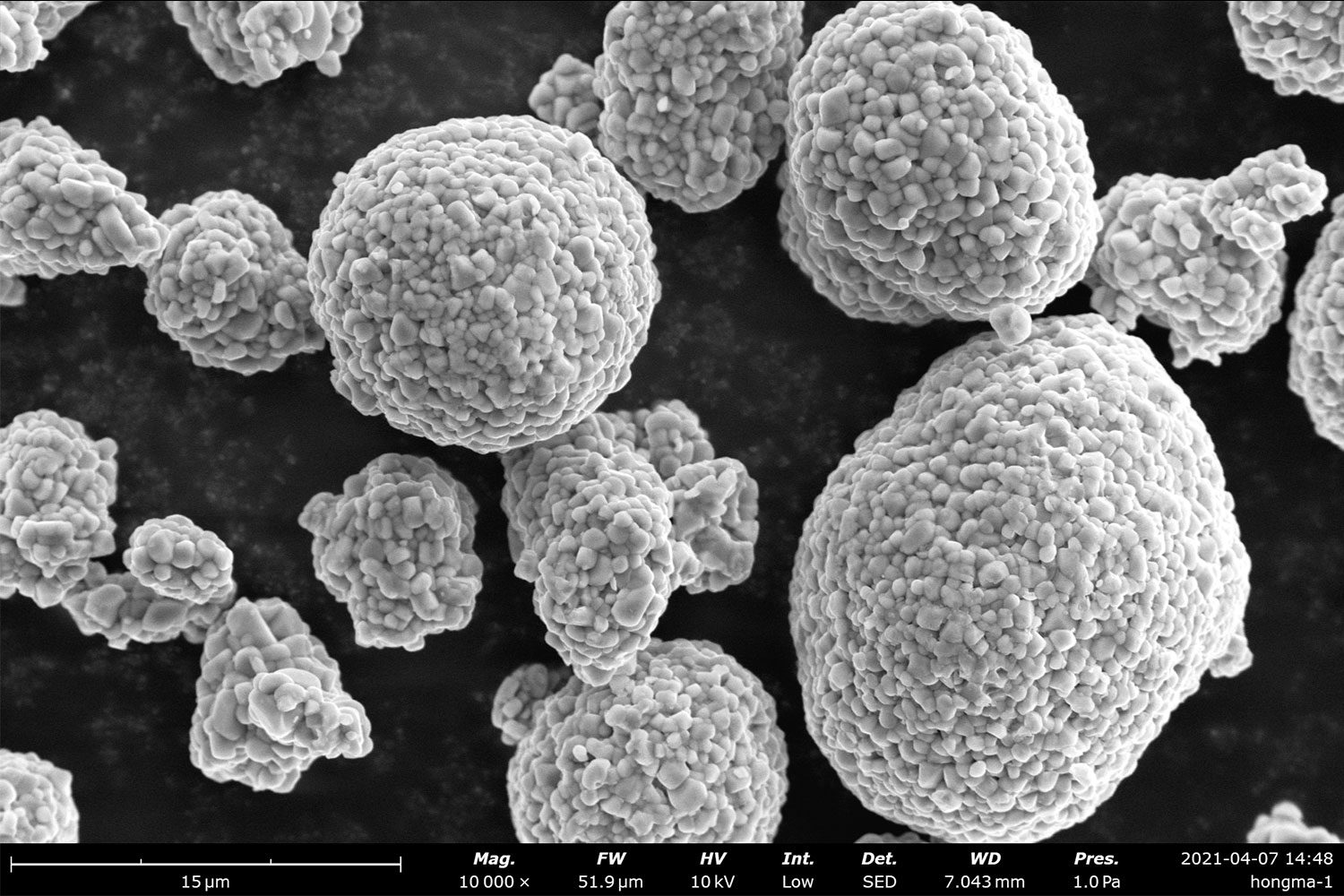
In the domain of scientific research and advanced industrial applications, the scanning electron microscope (SEM) is a powerful tool that has revolutionized our understanding of…
Posted: July 12, 2023 | Technology: Scanning Electron Microscopy
Scanning electron microscopy (SEM) is a powerful imaging technique where a focused beam of electrons is scanned over the surface of a sample for high-resolution…
Posted: June 28, 2023 | Technology: Scanning Electron Microscopy
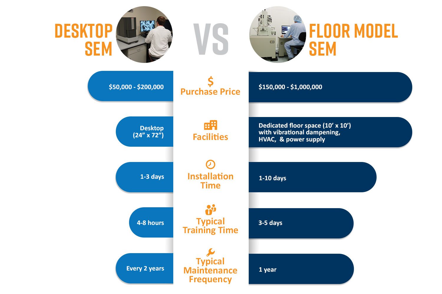
Purchasing a scanning electron microscope (SEM) can offer significant competitive advantage to organizations operating in a space where microscopy is paramount. An SEM uses a…
Posted: June 15, 2023 | Technology: Scanning Electron Microscopy
A scanning electron microscope (SEM) is a powerful scientific instrument used for high-resolution imaging and surface elemental analysis. They work by scanning a focused beam…
Posted: June 7, 2023 | Technology: Scanning Electron Microscopy
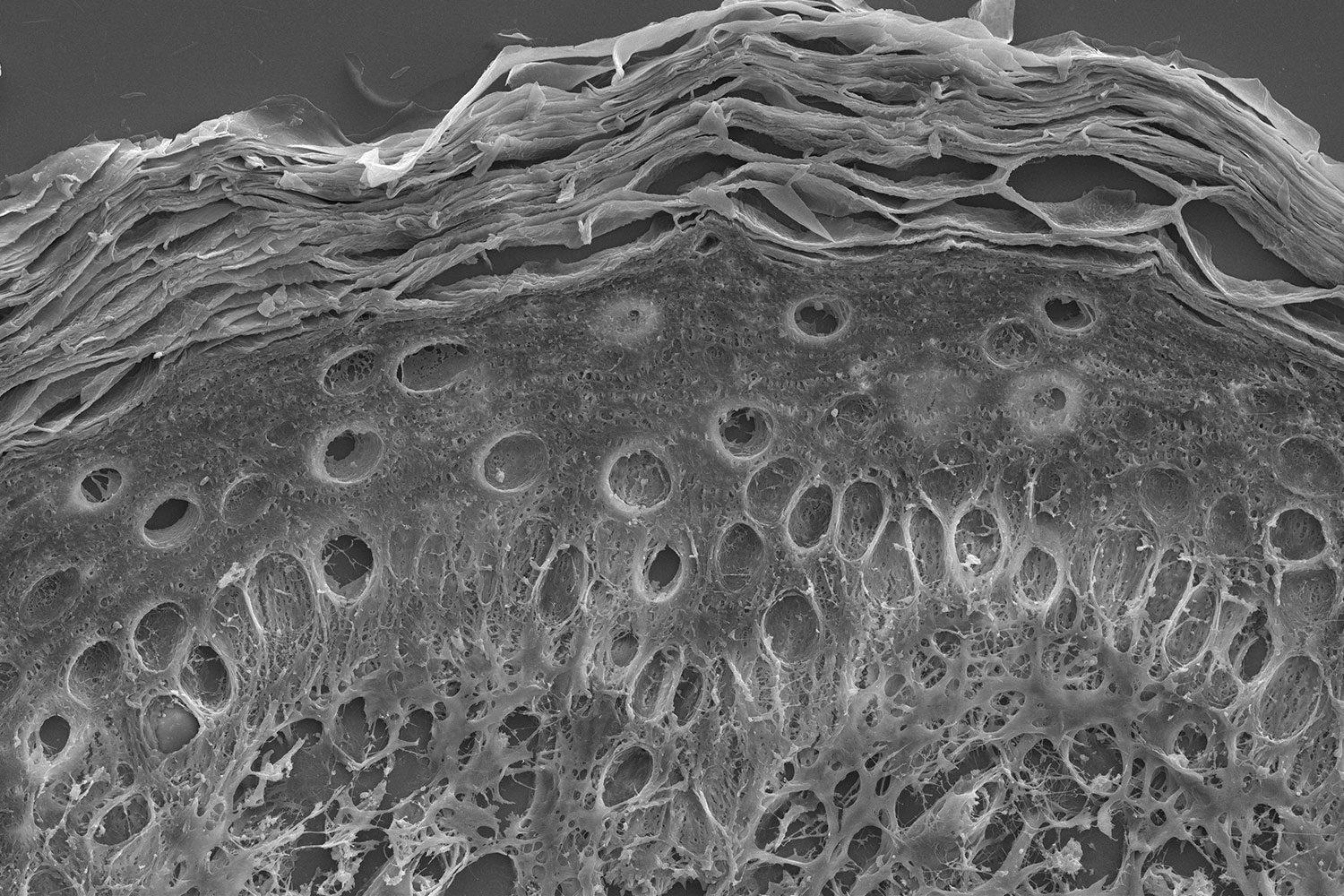
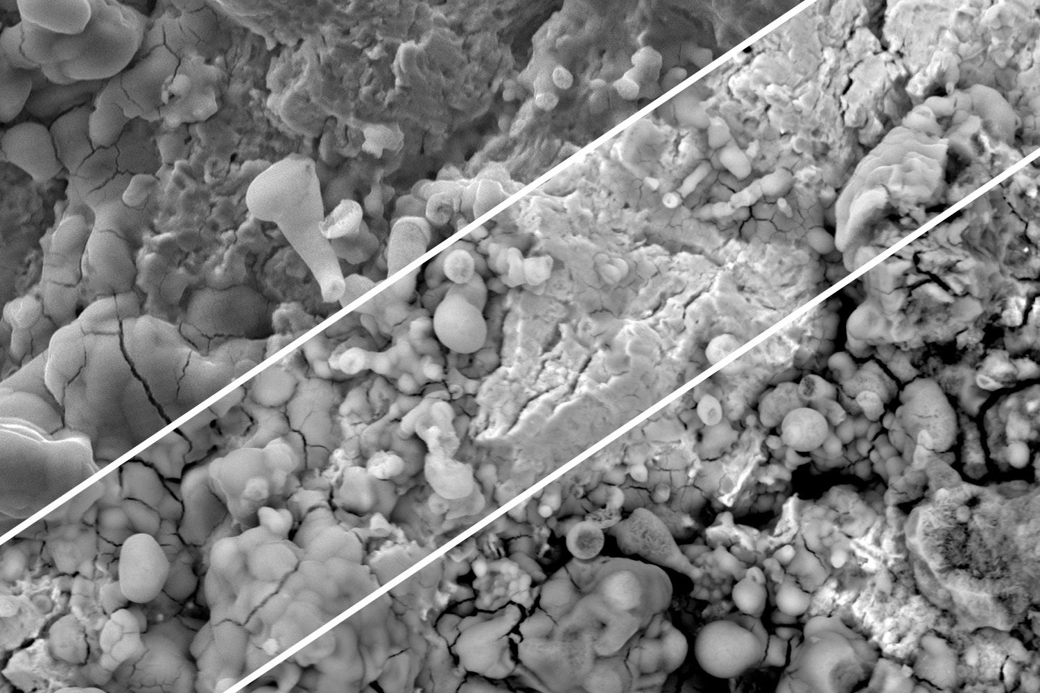
The skin is the ultimate barrier to the human body, protecting it from mechanical damage, radiation, extreme temperatures, and pathogens. The skin consists of three…
Posted: May 17, 2023 | Technology: Scanning Electron Microscopy
Scanning electron microscopy (SEM) is an extremely versatile analytical technique that produces high-resolution images by scanning a focused electron beam across a sample surface. Within…
Posted: April 19, 2023 | Technology: Scanning Electron Microscopy
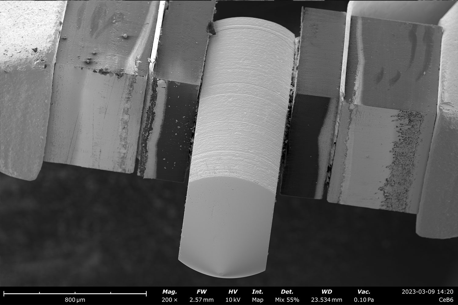
The electron source is one of the most important components of a scanning electron microscope (SEM) and is a major factor in determining its maximum…
Posted: March 28, 2023 | Technology: Scanning Electron Microscopy
The functional properties of a battery, not limited to just its performance, are inherently dependent upon the microstructure and surface morphology of electrodes and separators….
Posted: February 22, 2023 | Technology: Scanning Electron Microscopy