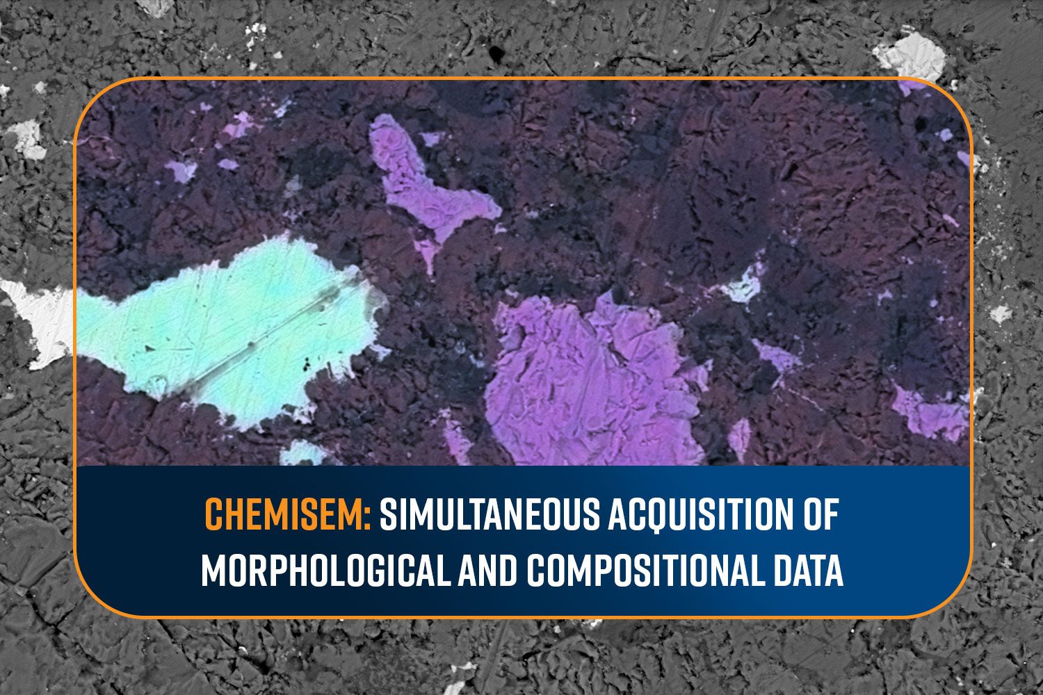
In a scanning electron microscope (SEM) with Energy Dispersive X-ray Spectroscopy (EDS), a sample’s elemental composition is identified via the X-rays emitted during the electron…
Posted: July 24, 2024 | Technology: Scanning Electron Microscopy

Energy Dispersive X-ray Spectroscopy (EDS) is an analytical technique used for elemental analysis and chemical characterization of materials. By detecting and measuring the energy of…
Posted: July 17, 2024 | Technology: Scanning Electron Microscopy
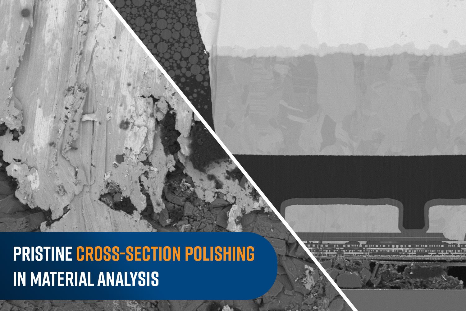
In material science, cross-section polishing is a critical method to enable the detailed examination of a sample material’s microstructure. This technique is essential for understanding…
Posted: July 10, 2024 | Technology: EM Sample Prep, Scanning Electron Microscopy
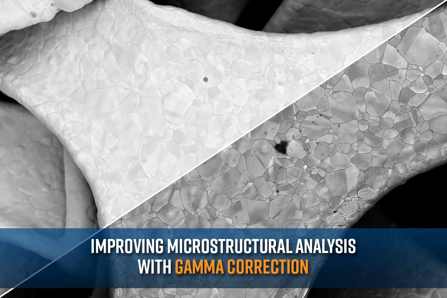
Scanning Electron Microscopy (SEM) is one of the most important tools in the arsenal of modern material science used to characterize micro and nanoscale features….
Posted: June 19, 2024 | Technology: Scanning Electron Microscopy
A scanning electron microscope (SEM) is capable of visualizing compositional heterogeneity on the surface of a sample by employing a backscattered electron detector (BSD). A…
Posted: May 22, 2024 | Technology: Scanning Electron Microscopy
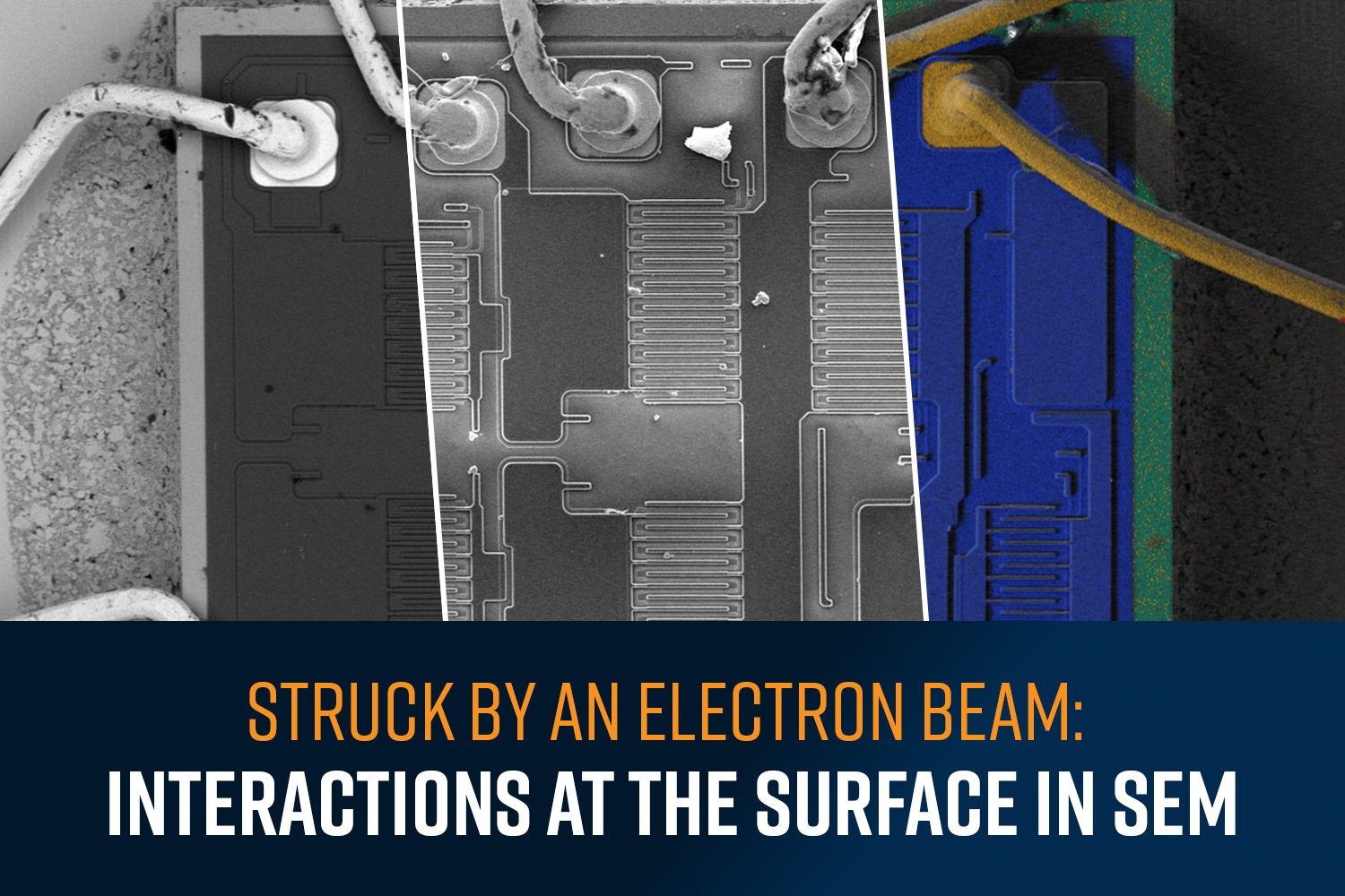
Scanning Electron Microscopy (SEM) generates high-resolution images by scanning a focused beam of electrons across the sample surface and detecting the signals produced through beam-sample…
Posted: May 8, 2024 | Technology: Scanning Electron Microscopy

Technical cleanliness is an analytical standard to determine the level of particulate contamination on machined parts. The goal of technical cleanliness is to characterize the…
Posted: May 2, 2024 | Technology: Scanning Electron Microscopy
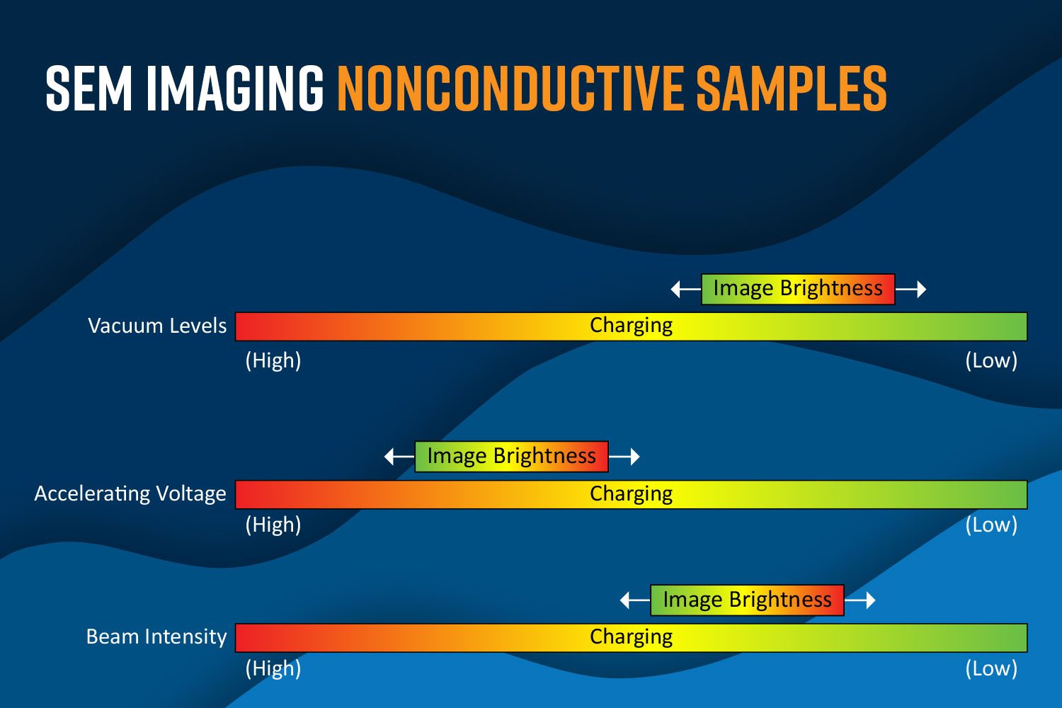
Charging is one of the most common issues when imaging non-conductive samples by scanning electron microscope (SEM) as it can distort images and damage the…
Posted: April 24, 2024 | Technology: Scanning Electron Microscopy
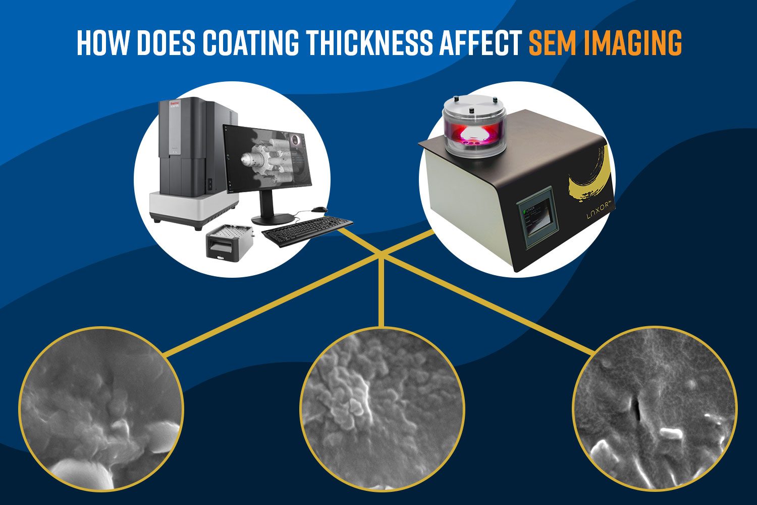
One of the most common challenges when analyzing non-conductive samples with a scanning electron microscope (SEM) is the charging effect. Without a conductive path, the…
Posted: April 18, 2024 | Technology: Scanning Electron Microscopy

Integrating the ability to perform high-resolution imaging and compositional analysis of materials into any laboratory becomes simplified with a desktop scanning electron microscope (SEM). In…
Posted: April 10, 2024 | Technology: Scanning Electron Microscopy

When acquiring a new scanning electron microscope (SEM), it can be challenging to identify a solution that not only delivers exceptional performance but also remains…
Posted: April 5, 2024 | Technology: Scanning Electron Microscopy

Precision manufacturing is a process that emphasizes exact specifications and extremely tight tolerances within fabricated components. Within this domain, the term technical cleanliness (TC) refers…
Posted: March 27, 2024 | Technology: Scanning Electron Microscopy