What Role Does SEM Play in Trace Evidence Analysis?
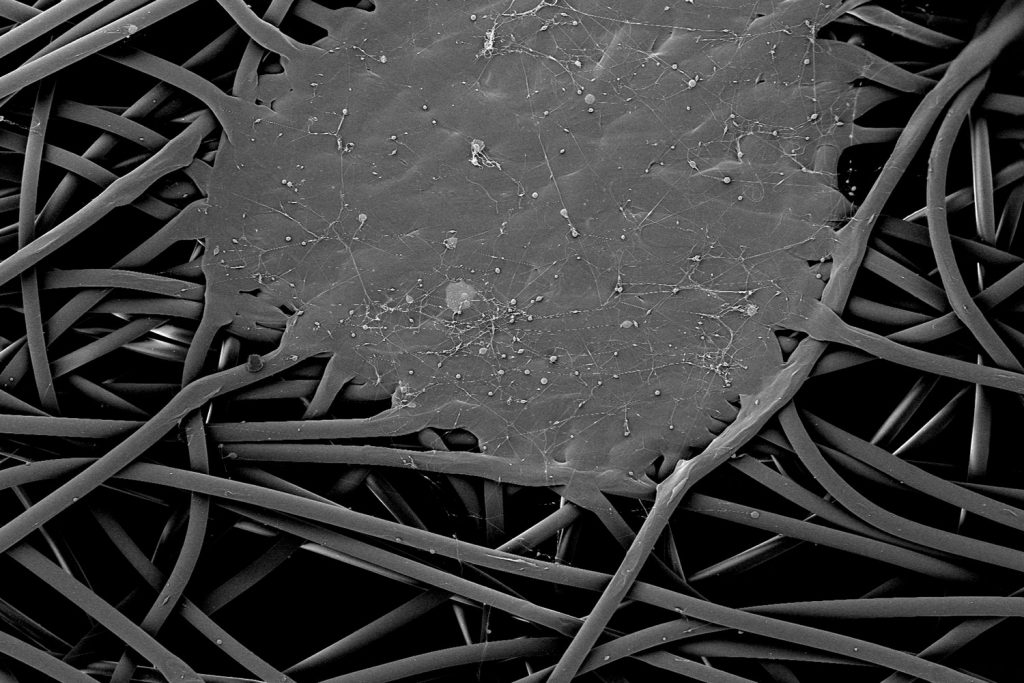
Scanning electron microscopy (SEM) is a powerful imaging technique where a focused beam of electrons is scanned over the surface of a sample for high-resolution analysis. SEM can offer detailed information regarding the morphology and the elemental composition of the surface. This can prove to be invaluable in the analysis of various types of evidence in forensic science.
American Crystallographic Association | July 7-11, 2023 | Baltimore, MD

73rd Annual Meeting of the American Crystallographic Association Come visit Booth #309 to discover solutions for streamlining your structural biology research workflows. Our technical experts will be here to discuss with you how the VitroJet can help you reduce cryo-EM grid preparation costs and help you solve 3D structures faster by controlling ice thickness. We […]
Microscopy and Microanalysis (M&M) 2023 | July 23-27, 2023 | Minneapolis, MN

Our booth is your gateway to unlock the full potential of your microscopy research. Stop by for live demonstrations of tabletop SEM/STEM and discover hybrid pixel detectors optimized for 4D-STEM, modular CL detectors, ion mills, sputter coaters, and cryo-EM sample preparation solutions. For over two decades, we have been committed to your success.
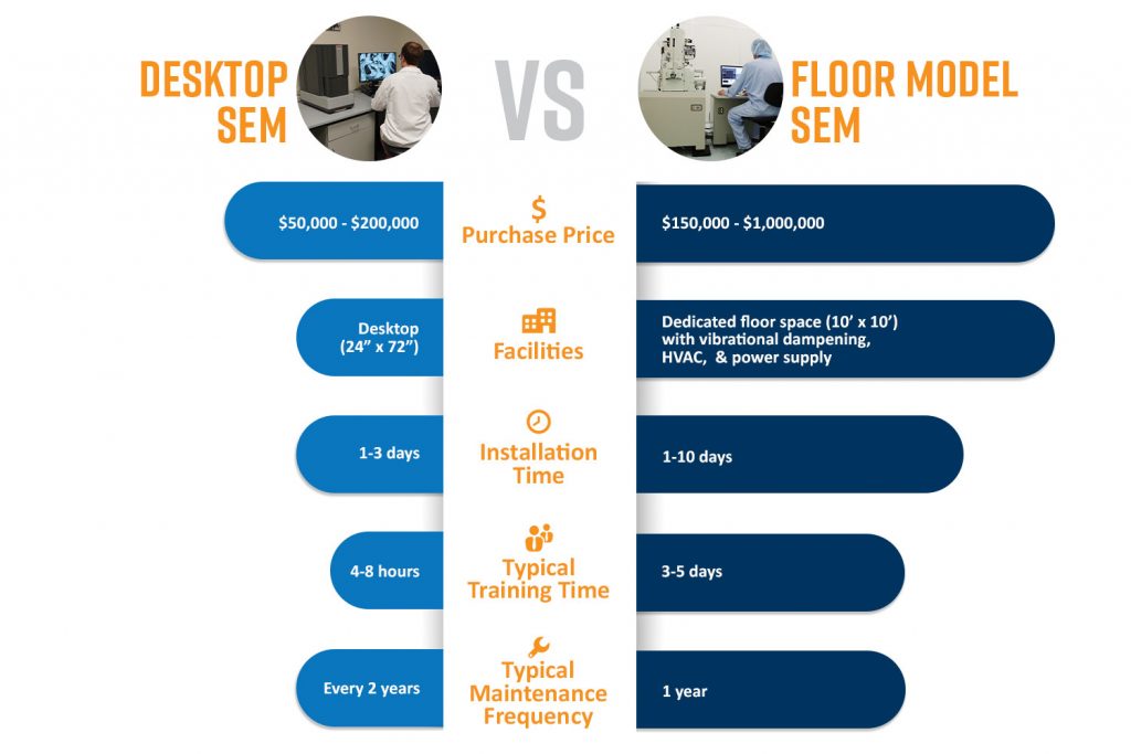
8 Factors to Consider when Purchasing a Scanning Electron Microscope (SEM)
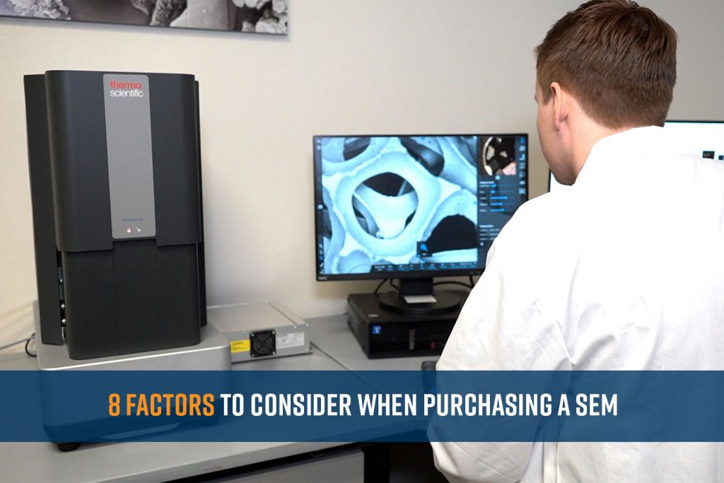
Purchasing a scanning electron microscope (SEM) can offer significant competitive advantage to organizations operating in a space where microscopy is paramount. An SEM uses a focused beam of electrons to generate high resolution images by scanning it across a sample surface. The technique is far superior to optical microscopy in terms of resolution, magnification, and […]
How Much Does a Scanning Electron Microscope (SEM) Cost?
A scanning electron microscope (SEM) is a powerful scientific instrument used for high-resolution imaging and surface elemental analysis. They work by scanning a focused beam of electrons across the sample’s surface and detecting the resulting signals to create detailed images. SEMs provide value in a wide range of applications including materials science, biology, nanotechnology, forensics, […]
Visualizing Skin Tissue Morphology with Scanning Electron Microscopy
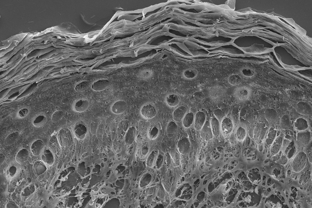
The skin is the ultimate barrier to the human body, protecting it from mechanical damage, radiation, extreme temperatures, and pathogens. The skin consists of three layers: the epidermis (outer layer), dermis (middle), and hypodermis (inner layer). Each layer serves a distinct purpose. The epidermis provides the primary barrier whereas the dermis and hypodermis contain hair follicles, sweat glands, connective tissue, and fat to provide mechanical strength and warmth to our bodies. During minor injuries, the skin can normally regenerate the damaged areas on its own. In cases of extensive injuries, such as through disease or burn wounds, the skin is unable to regenerate on its own which leads to scar tissue formation or in worst cases, chronic wounds that need medical attention.
Using the Phenom Desktop SEM for Quality Control at Menlo Micro

“We discovered Phenom has the best value with results close to a full-size SEM” – Dr Naomi C., Menlo Micro
On occasion, we are given the opportunity to watch, learn, and broadcast some of the most fascinating inventions of our time. Today is that day of sharing.
The Air Water Interface and Sample Preparation for Cryo-EM
The air-water interface (AWI) is essentially the chaotic boundary where a solution meets the air. When protein molecules in solution contact the AWI, they tend to align themselves along the interface with the hydrophilic regions facing inward towards the water environment and the hydrophobic regions facing outwards towards the air environment. The AWI presents one […]
Workflow Automation in SEM Analysis

Scanning electron microscopy (SEM) is an extremely versatile analytical technique that produces high-resolution images by scanning a focused electron beam across a sample surface. Within the SEM, multiple detectors capture different signals generated through beam-sample interactions so that surface morphology and elemental composition can be visualized at nanometer resolution. The superior resolving power of SEMs […]
Which Electron Source is Best?
The electron source is one of the most important components of a scanning electron microscope (SEM) and is a major factor in determining its maximum analytical performance. There are three common types of electron sources found in SEMs: tungsten filaments, solid state hexaboride crystals, and field emission guns. How do electron sources work? As the […]